ZHCSBY9G July 2013 – June 2021 TPS54561
PRODUCTION DATA
- 1 特性
- 2 应用
- 3 说明
- 4 Revision History
- 5 Pin Configuration and Functions
- 6 Specifications
-
7 Detailed Description
- 7.1 Overview
- 7.2 Functional Block Diagram
- 7.3
Feature Description
- 7.3.1 Fixed Frequency PWM Control
- 7.3.2 Slope Compensation Output Current
- 7.3.3 Pulse Skip Eco-mode
- 7.3.4 Low Dropout Operation and Bootstrap Voltage (BOOT)
- 7.3.5 Error Amplifier
- 7.3.6 Adjusting the Output Voltage
- 7.3.7 Enable and Adjusting Undervoltage Lockout
- 7.3.8 Soft Start/Tracking Pin (SS/TR)
- 7.3.9 Sequencing
- 7.3.10 Constant Switching Frequency and Timing Resistor (RT/CLK) Pin)
- 7.3.11 Maximum Switching Frequency
- 7.3.12 Synchronization to RT/CLK Pin
- 7.3.13 Accurate Current Limit Operation
- 7.3.14 Power Good (PWRGD Pin)
- 7.3.15 Overvoltage Protection
- 7.3.16 Thermal Shutdown
- 7.3.17 Small Signal Model for Loop Response
- 7.3.18 Simple Small Signal Model for Peak Current Mode Control
- 7.3.19 Small Signal Model for Frequency Compensation
- 7.4 Device Functional Modes
-
8 Application and Implementation
- 8.1 Application Information
- 8.2
Typical Applications
- 8.2.1
Buck Converter for 7-V to 60-V Input to 5-V at 5-A Output
- 8.2.1.1 Design Requirements
- 8.2.1.2
Detailed Design Procedure
- 8.2.1.2.1 Custom Design with WEBENCH® Tools
- 8.2.1.2.2 Selecting the Switching Frequency
- 8.2.1.2.3 Output Inductor Selection (LO)
- 8.2.1.2.4 Output Capacitor
- 8.2.1.2.5 Catch Diode
- 8.2.1.2.6 Input Capacitor
- 8.2.1.2.7 Slow Start Capacitor
- 8.2.1.2.8 Bootstrap Capacitor Selection
- 8.2.1.2.9 Undervoltage Lockout Set Point
- 8.2.1.2.10 Output Voltage and Feedback Resistors Selection
- 8.2.1.2.11 Compensation
- 8.2.1.2.12 Power Dissipation Estimate
- 8.2.1.2.13 Safe Operating Area
- 8.2.1.2.14 Discontinuous Conduction Mode and Eco-mode Boundary
- 8.2.1.3 Application Curves
- 8.2.2 Inverting Buck-Boost Topology for Positive Input to Negative Output
- 8.2.3 Split-Rail Topology for Positive Input to Negative and Positive Output
- 8.2.1
Buck Converter for 7-V to 60-V Input to 5-V at 5-A Output
- 9 Power Supply Recommendations
- 10Layout
- 11Device and Documentation Support
- 12Mechanical, Packaging, and Orderable Information
8.2.1.2.6 Input Capacitor
The TPS54561 requires a high quality ceramic type X5R or X7R input decoupling capacitor with at least 3 μF of effective capacitance. Some applications will benefit from additional bulk capacitance. The effective capacitance includes any loss of capacitance due to dc bias effects. The voltage rating of the input capacitor must be greater than the maximum input voltage. The capacitor must also have a ripple current rating greater than the maximum input current ripple of the TPS54561. The input ripple current can be calculated using Equation 41.
The value of a ceramic capacitor varies significantly with temperature and the dc bias applied to the capacitor. The capacitance variations due to temperature can be minimized by selecting a dielectric material that is more stable over temperature. X5R and X7R ceramic dielectrics are usually selected for switching regulator capacitors because they have a high capacitance to volume ratio and are fairly stable over temperature. The input capacitor must also be selected with consideration for the dc bias. The effective value of a capacitor decreases as the dc bias across a capacitor increases.
For this example design, a ceramic capacitor with at least a 60 V voltage rating is required to support the maximum input voltage. Common standard ceramic capacitor voltage ratings include 4 V, 6.3 V, 10 V, 16 V, 25 V, 50 V or 100 V. For this example, four 2.2 μF, 100 V capacitors in parallel are used. Table 8-2 shows several choices of high voltage capacitors.
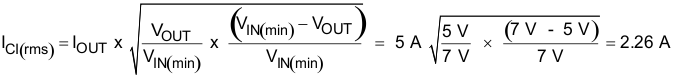
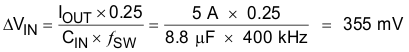
The input capacitance value determines the input ripple voltage of the regulator. The input voltage ripple can be calculated using Equation 42. Using the design example values, IOUT = 5 A, CIN = 8.8 μF, ƒsw = 400 kHz, yields an input voltage ripple of 355 mV and a rms input ripple current of 2.26 A.
| VENDOR | VALUE (μF) | EIA Size | VOLTAGE | DIALECTRIC | COMMENTS |
|---|---|---|---|---|---|
| Murata | 1 to 2.2 | 1210 | 100 V | X7R | GRM32 series |
| 1 to 4.7 | 50 V | ||||
| 1 | 1206 | 100 V | GRM31 series | ||
| 1 to 2.2 | 50 V | ||||
| Vishay | 1 to 1.8 | 2220 | 50 V | VJ X7R series | |
| 1 to 1.2 | 100 V | ||||
| 1 to 3.9 | 2225 | 50 V | |||
| 1 to 1.8 | 100 V | ||||
| TDK | 1 to 2.2 | 1812 | 100 V | C series C4532 | |
| 1.5 to 6.8 | 50 V | ||||
| 1 to 2.2 | 1210 | 100 V | C series C3225 | ||
| 1 to 3.3 | 50 V | ||||
| AVX | 1 to 4.7 | 1210 | 50 V | X7R dielectric series | |
| 1 | 100 V | ||||
| 1 to 4.7 | 1812 | 50 V | |||
| 1 to 2.2 | 100 V |