ZHCSBY9G July 2013 – June 2021 TPS54561
PRODUCTION DATA
- 1 特性
- 2 应用
- 3 说明
- 4 Revision History
- 5 Pin Configuration and Functions
- 6 Specifications
-
7 Detailed Description
- 7.1 Overview
- 7.2 Functional Block Diagram
- 7.3
Feature Description
- 7.3.1 Fixed Frequency PWM Control
- 7.3.2 Slope Compensation Output Current
- 7.3.3 Pulse Skip Eco-mode
- 7.3.4 Low Dropout Operation and Bootstrap Voltage (BOOT)
- 7.3.5 Error Amplifier
- 7.3.6 Adjusting the Output Voltage
- 7.3.7 Enable and Adjusting Undervoltage Lockout
- 7.3.8 Soft Start/Tracking Pin (SS/TR)
- 7.3.9 Sequencing
- 7.3.10 Constant Switching Frequency and Timing Resistor (RT/CLK) Pin)
- 7.3.11 Maximum Switching Frequency
- 7.3.12 Synchronization to RT/CLK Pin
- 7.3.13 Accurate Current Limit Operation
- 7.3.14 Power Good (PWRGD Pin)
- 7.3.15 Overvoltage Protection
- 7.3.16 Thermal Shutdown
- 7.3.17 Small Signal Model for Loop Response
- 7.3.18 Simple Small Signal Model for Peak Current Mode Control
- 7.3.19 Small Signal Model for Frequency Compensation
- 7.4 Device Functional Modes
-
8 Application and Implementation
- 8.1 Application Information
- 8.2
Typical Applications
- 8.2.1
Buck Converter for 7-V to 60-V Input to 5-V at 5-A Output
- 8.2.1.1 Design Requirements
- 8.2.1.2
Detailed Design Procedure
- 8.2.1.2.1 Custom Design with WEBENCH® Tools
- 8.2.1.2.2 Selecting the Switching Frequency
- 8.2.1.2.3 Output Inductor Selection (LO)
- 8.2.1.2.4 Output Capacitor
- 8.2.1.2.5 Catch Diode
- 8.2.1.2.6 Input Capacitor
- 8.2.1.2.7 Slow Start Capacitor
- 8.2.1.2.8 Bootstrap Capacitor Selection
- 8.2.1.2.9 Undervoltage Lockout Set Point
- 8.2.1.2.10 Output Voltage and Feedback Resistors Selection
- 8.2.1.2.11 Compensation
- 8.2.1.2.12 Power Dissipation Estimate
- 8.2.1.2.13 Safe Operating Area
- 8.2.1.2.14 Discontinuous Conduction Mode and Eco-mode Boundary
- 8.2.1.3 Application Curves
- 8.2.2 Inverting Buck-Boost Topology for Positive Input to Negative Output
- 8.2.3 Split-Rail Topology for Positive Input to Negative and Positive Output
- 8.2.1
Buck Converter for 7-V to 60-V Input to 5-V at 5-A Output
- 9 Power Supply Recommendations
- 10Layout
- 11Device and Documentation Support
- 12Mechanical, Packaging, and Orderable Information
8.2.1.2.7 Slow Start Capacitor
The slow start capacitor determines the minimum amount of time it will take for the output voltage to reach its nominal programmed value during power up. This is useful if a load requires a controlled voltage slew rate. This is also used if the output capacitance is large and would require large amounts of current to quickly charge the capacitor to the output voltage level. The large currents necessary to charge the capacitor may make the TPS54561 reach the current limit or excessive current draw from the input power supply may cause the input voltage rail to sag. Limiting the output voltage slew rate solves both of these problems.
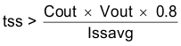
The slow start time must be long enough to allow the regulator to charge the output capacitor up to the output voltage without drawing excessive current. Equation 43 can be used to find the minimum slow start time, tss, necessary to charge the output capacitor, Cout, from 10% to 90% of the output voltage, Vout, with an average slow start current of Issavg. In the example, to charge the effective output capacitance of 87 µF up to 5 V with an average current of 1 A requires a 0.3 ms slow start time.
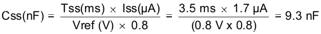
Once the slow start time is known, the slow start capacitor value can be calculated using Equation 5. For the example circuit, the slow start time is not too critical since the output capacitor value is 3 x 47 μF which does not require much current to charge to 5 V. The example circuit has the slow start time set to an arbitrary value of 3.5 ms which requires a 9.3-nF slow start capacitor calculated by Equation 44. For this design, the next larger standard value of 10 nF is used.