ZHCSBY9G July 2013 – June 2021 TPS54561
PRODUCTION DATA
- 1 特性
- 2 应用
- 3 说明
- 4 Revision History
- 5 Pin Configuration and Functions
- 6 Specifications
-
7 Detailed Description
- 7.1 Overview
- 7.2 Functional Block Diagram
- 7.3
Feature Description
- 7.3.1 Fixed Frequency PWM Control
- 7.3.2 Slope Compensation Output Current
- 7.3.3 Pulse Skip Eco-mode
- 7.3.4 Low Dropout Operation and Bootstrap Voltage (BOOT)
- 7.3.5 Error Amplifier
- 7.3.6 Adjusting the Output Voltage
- 7.3.7 Enable and Adjusting Undervoltage Lockout
- 7.3.8 Soft Start/Tracking Pin (SS/TR)
- 7.3.9 Sequencing
- 7.3.10 Constant Switching Frequency and Timing Resistor (RT/CLK) Pin)
- 7.3.11 Maximum Switching Frequency
- 7.3.12 Synchronization to RT/CLK Pin
- 7.3.13 Accurate Current Limit Operation
- 7.3.14 Power Good (PWRGD Pin)
- 7.3.15 Overvoltage Protection
- 7.3.16 Thermal Shutdown
- 7.3.17 Small Signal Model for Loop Response
- 7.3.18 Simple Small Signal Model for Peak Current Mode Control
- 7.3.19 Small Signal Model for Frequency Compensation
- 7.4 Device Functional Modes
-
8 Application and Implementation
- 8.1 Application Information
- 8.2
Typical Applications
- 8.2.1
Buck Converter for 7-V to 60-V Input to 5-V at 5-A Output
- 8.2.1.1 Design Requirements
- 8.2.1.2
Detailed Design Procedure
- 8.2.1.2.1 Custom Design with WEBENCH® Tools
- 8.2.1.2.2 Selecting the Switching Frequency
- 8.2.1.2.3 Output Inductor Selection (LO)
- 8.2.1.2.4 Output Capacitor
- 8.2.1.2.5 Catch Diode
- 8.2.1.2.6 Input Capacitor
- 8.2.1.2.7 Slow Start Capacitor
- 8.2.1.2.8 Bootstrap Capacitor Selection
- 8.2.1.2.9 Undervoltage Lockout Set Point
- 8.2.1.2.10 Output Voltage and Feedback Resistors Selection
- 8.2.1.2.11 Compensation
- 8.2.1.2.12 Power Dissipation Estimate
- 8.2.1.2.13 Safe Operating Area
- 8.2.1.2.14 Discontinuous Conduction Mode and Eco-mode Boundary
- 8.2.1.3 Application Curves
- 8.2.2 Inverting Buck-Boost Topology for Positive Input to Negative Output
- 8.2.3 Split-Rail Topology for Positive Input to Negative and Positive Output
- 8.2.1
Buck Converter for 7-V to 60-V Input to 5-V at 5-A Output
- 9 Power Supply Recommendations
- 10Layout
- 11Device and Documentation Support
- 12Mechanical, Packaging, and Orderable Information
8.2.1.2.4 Output Capacitor
There are three primary considerations for selecting the value of the output capacitor. The output capacitor determines the modulator pole, the output voltage ripple, and how the regulator responds to a large change in load current. The output capacitance needs to be selected based on the most stringent of these three criteria.
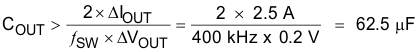
The desired response to a large change in the load current is the first criteria. The output capacitor needs to supply the increased load current until the regulator responds to the load step. The regulator does not respond immediately to a large, fast increase in the load current such as transitioning from no load to a full load. The regulator usually needs two or more clock cycles for the control loop to sense the change in output voltage and adjust the peak switch current in response to the higher load. The output capacitance must be large enough to supply the difference in current for 2 clock cycles to maintain the output voltage within the specified range. Equation 35 shows the minimum output capacitance necessary, where ΔIOUT is the change in output current, ƒsw is the regulators switching frequency and ΔVOUT is the allowable change in the output voltage. For this example, the transient load response is specified as a 4% change in VOUT for a load step from 1.25 A to 3.75 A. Therefore, ΔIOUT is 3.75 A - 1.25 A = 2.5 A and ΔVOUT = 0.04 × 5 = 0.2 V. Using these numbers gives a minimum capacitance of 62.5 μF. This value does not take the ESR of the output capacitor into account in the output voltage change. For ceramic capacitors, the ESR is usually small enough to be ignored. Aluminum electrolytic and tantalum capacitors have higher ESR that must be included in load step calculations.
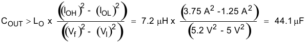
The output capacitor must also be sized to absorb energy stored in the inductor when transitioning from a high to low load current. The catch diode of the regulator cannot sink current so energy stored in the inductor can produce an output voltage overshoot when the load current rapidly decreases. A typical load step response is shown in Figure 8-6. The excess energy absorbed in the output capacitor will increase the voltage on the capacitor. The capacitor must be sized to maintain the desired output voltage during these transient periods. Equation 36 calculates the minimum capacitance required to keep the output voltage overshoot to a desired value, where LO is the value of the inductor, IOH is the output current under heavy load, IOL is the output under light load, Vf is the peak output voltage, and Vi is the initial voltage. For this example, the worst case load step will be from 3.75 A to 1.25 A. The output voltage increases during this load transition and the stated maximum in our specification is 4 % of the output voltage. This makes Vf = 1.04 × 5 = 5.2. Vi is the initial capacitor voltage which is the nominal output voltage of 5 V. Using these numbers in Equation 36 yields a minimum capacitance of
44.1 μF.
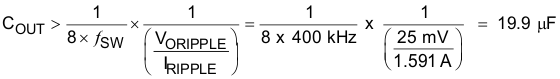
Equation 37 calculates the minimum output capacitance needed to meet the output voltage ripple specification, where ƒsw is the switching frequency, VORIPPLE is the maximum allowable output voltage ripple, and IRIPPLE is the inductor ripple current. Equation 37 yields 19.9 μF.
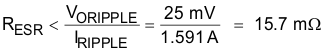
Equation 38 calculates the maximum ESR an output capacitor can have to meet the output voltage ripple specification. Equation 38 indicates the ESR should be less than 15.7 mΩ.
The most stringent criteria for the output capacitor is 62.5 μF required to maintain the output voltage within regulation tolerance during a load transient.
Capacitance de-ratings for aging, temperature and dc bias increases this minimum value. For this example, 3 x 47 μF, 10-V ceramic capacitors with 5 mΩ of ESR will be used. The derated capacitance is 87.4 µF, well above the minimum required capacitance of 62.5 µF.
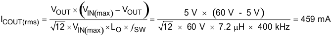
Capacitors are generally rated for a maximum ripple current that can be filtered without degrading capacitor reliability. Some capacitor data sheets specify the Root Mean Square (RMS) value of the maximum ripple current. Equation 39 can be used to calculate the RMS ripple current that the output capacitor must support. For this example, Equation 39 yields 459 mA.