ZHCSBY9G July 2013 – June 2021 TPS54561
PRODUCTION DATA
- 1 特性
- 2 应用
- 3 说明
- 4 Revision History
- 5 Pin Configuration and Functions
- 6 Specifications
-
7 Detailed Description
- 7.1 Overview
- 7.2 Functional Block Diagram
- 7.3
Feature Description
- 7.3.1 Fixed Frequency PWM Control
- 7.3.2 Slope Compensation Output Current
- 7.3.3 Pulse Skip Eco-mode
- 7.3.4 Low Dropout Operation and Bootstrap Voltage (BOOT)
- 7.3.5 Error Amplifier
- 7.3.6 Adjusting the Output Voltage
- 7.3.7 Enable and Adjusting Undervoltage Lockout
- 7.3.8 Soft Start/Tracking Pin (SS/TR)
- 7.3.9 Sequencing
- 7.3.10 Constant Switching Frequency and Timing Resistor (RT/CLK) Pin)
- 7.3.11 Maximum Switching Frequency
- 7.3.12 Synchronization to RT/CLK Pin
- 7.3.13 Accurate Current Limit Operation
- 7.3.14 Power Good (PWRGD Pin)
- 7.3.15 Overvoltage Protection
- 7.3.16 Thermal Shutdown
- 7.3.17 Small Signal Model for Loop Response
- 7.3.18 Simple Small Signal Model for Peak Current Mode Control
- 7.3.19 Small Signal Model for Frequency Compensation
- 7.4 Device Functional Modes
-
8 Application and Implementation
- 8.1 Application Information
- 8.2
Typical Applications
- 8.2.1
Buck Converter for 7-V to 60-V Input to 5-V at 5-A Output
- 8.2.1.1 Design Requirements
- 8.2.1.2
Detailed Design Procedure
- 8.2.1.2.1 Custom Design with WEBENCH® Tools
- 8.2.1.2.2 Selecting the Switching Frequency
- 8.2.1.2.3 Output Inductor Selection (LO)
- 8.2.1.2.4 Output Capacitor
- 8.2.1.2.5 Catch Diode
- 8.2.1.2.6 Input Capacitor
- 8.2.1.2.7 Slow Start Capacitor
- 8.2.1.2.8 Bootstrap Capacitor Selection
- 8.2.1.2.9 Undervoltage Lockout Set Point
- 8.2.1.2.10 Output Voltage and Feedback Resistors Selection
- 8.2.1.2.11 Compensation
- 8.2.1.2.12 Power Dissipation Estimate
- 8.2.1.2.13 Safe Operating Area
- 8.2.1.2.14 Discontinuous Conduction Mode and Eco-mode Boundary
- 8.2.1.3 Application Curves
- 8.2.2 Inverting Buck-Boost Topology for Positive Input to Negative Output
- 8.2.3 Split-Rail Topology for Positive Input to Negative and Positive Output
- 8.2.1
Buck Converter for 7-V to 60-V Input to 5-V at 5-A Output
- 9 Power Supply Recommendations
- 10Layout
- 11Device and Documentation Support
- 12Mechanical, Packaging, and Orderable Information
8.2.1.2.2 Selecting the Switching Frequency
The first step is to choose a switching frequency for the regulator. Typically, the designer uses the highest switching frequency possible since this produces the smallest solution size. High switching frequency allows for lower value inductors and smaller output capacitors compared to a power supply that switches at a lower frequency. The switching frequency that can be selected is limited by the minimum on-time of the internal power switch, the input voltage, the output voltage and the frequency foldback protection.
Equation 12 and Equation 13 should be used to calculate the upper limit of the switching frequency for the regulator. Choose the lower value result from the two equations. Switching frequencies higher than these values results in pulse skipping or the lack of overcurrent protection during a short circuit.
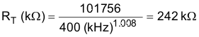
The typical minimum on time, tonmin, is 135 ns for the TPS54561. For this example, the output voltage is 5 V and the maximum input voltage is 60 V, which allows for a maximum switch frequency up to 708 kHz to avoid pulse skipping from Equation 12. To ensure overcurrent runaway is not a concern during short circuits use Equation 13 to determine the maximum switching frequency for frequency foldback protection. With a maximum input voltage of 60 V, assuming a diode voltage of 0.7 V, inductor resistance of 11 mΩ, switch resistance of 87 mΩ, a current limit value of 6 A and short circuit output voltage of 0.1 V, the maximum switching frequency is 855 kHz.
For this design, a lower switching frequency of 400 kHz is chosen to operate comfortably below the calculated maximums. To determine the timing resistance for a given switching frequency, use Equation 10 or the curve in Figure 6-6. The switching frequency is set by resistor R3 shown in Figure 8-1. For 400-kHz operation, the closest standard value resistor is 243 kΩ.