ZHCSUI2E May 2006 – January 2024 TPS28225
PRODUCTION DATA
- 1
- 1 特性
- 2 应用
- 3 说明
- 4 Pin Configuration and Functions
- 5 Specifications
- 6 Detailed Description
- 7 Application and Implementation
- 8 Power Supply Recommendations
- 9 Layout
- 10Device and Documentation Support
- 11Revision History
- 12Mechanical, Packaging, and Orderable Information
封装选项
机械数据 (封装 | 引脚)
散热焊盘机械数据 (封装 | 引脚)
- DRB|8
订购信息
4 Pin Configuration and Functions
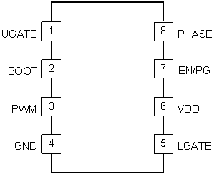
 Figure 4-1 D
Package8-Pin SOICTop View
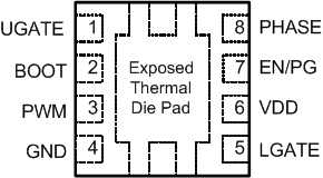
 Figure 4-2 DRB Package8-Pin VSONTop View
Table 4-1 Pin Functions
| PIN | I/O | DESCRIPTION | ||
|---|---|---|---|---|
| NAME | NO. | |||
| SOIC | VSON | |||
| BOOT | 2 | 2 | I/O | Floating bootstrap supply pin for the upper gate drive. Connect the bootstrap capacitor between this pin and the Phase pin. The bootstrap capacitor provides the charge to turn on the upper MOSFET. |
| EN/PG | 7 | 7 | I/O | Enable/power good input/output pin with 1-MΩ impedance. Connect this pin to High to enable and Low to disable the device. When disabled, the device draws less than 350-μA bias current. If the VDD is below UVLO threshold or over temperature shutdown occurs, this pin is internally pulled low. |
| GND | 4 | 4 | – | Ground pin. All signals are referenced to this node. |
| LGATE | 5 | 5 | O | Lower gate drive sink and source output. Connect to the gate of the low-side power N-Channel MOSFET. |
| PHASE | 8 | 8 | I | Connect this pin to the source of the upper MOSFET and the drain of the lower MOSFET. This pin provides a return path for the upper gate driver. |
| PWM | 3 | 3 | I | The PWM signal is the control input for the driver. The PWM signal can enter three distinct states during operation, see the 3-state PWM Input section under DETAILED DESCRIPTION for further details. Connect this pin to the PWM output of the controller. |
| Thermal pad | Exposed die pad | – | Connect directly to the GND for better thermal performance and EMI. | |
| UGATE | 1 | 1 | O | Upper gate drive sink/source output. Connect to gate of high-side power N-Channel MOSFET. |
| VDD | 6 | 6 | I | Connect this pin to a 5-V bias supply. Place a high quality bypass capacitor from this pin to GND. |