ZHCSI22F October   2017  – December 2021 TPS2662

PRODUCTION DATA  

  1. 特性
  2. 应用
  3. 说明
  4. Revision History
  5. Device Comparison Table
  6. Pin Configuration and Functions
  7. Specifications
    1. 7.1 Absolute Maximum Ratings
    2. 7.2 ESD Ratings
    3. 7.3 Recommended Operating Conditions
    4. 7.4 Thermal Information
    5. 7.5 Electrical Characteristics
    6. 7.6 Timing Requirements
    7. 7.7 Typical Characteristics
  8. Parameter Measurement Information
  9. Detailed Description
    1. 9.1 Overview
    2. 9.2 Functional Block Diagram
    3. 9.3 Feature Description
      1. 9.3.1 Undervoltage Lockout (UVLO)
      2. 9.3.2 Overvoltage Protection (OVP)
      3. 9.3.3 Hot Plug-In and Inrush Current Control
      4. 9.3.4 Reverse Polarity Protection
        1. 9.3.4.1 Input Side Reverse Polarity Protection
        2. 9.3.4.2 Output Side Reverse Polarity Protection
      5. 9.3.5 Overload and Short-Circuit Protection
        1. 9.3.5.1 Overload Protection
        2.       28
        3. 9.3.5.2 Short-Circuit Protection
          1. 9.3.5.2.1 Start-Up With Short-Circuit On Output
      6. 9.3.6 Reverse Current Protection
      7. 9.3.7 FAULT Response
      8. 9.3.8 IN, OUT, RTN, and GND Pins
      9. 9.3.9 Thermal Shutdown
    4. 9.4 Device Functional Modes
      1. 9.4.1 Low Current Shutdown Control (SHDN)
  10. 10Application and Implementation
    1. 10.1 Application Information
    2. 10.2 Typical Application
      1. 10.2.1 Design Requirements
      2. 10.2.2 Detailed Design Procedure
        1. 10.2.2.1 Step-by-Step Design Procedure
        2. 10.2.2.2 Programming the Current Limit Threshold R(ILIM) Selection
        3. 10.2.2.3 Undervoltage Lockout and Overvoltage Set Point
        4. 10.2.2.4 Setting Output Voltage Ramp Time—(tdVdT)
          1. 10.2.2.4.1 Case 1: Start-Up Without Load—Only Output Capacitance C(OUT) Draws Current During Start-Up
          2. 10.2.2.4.2 Case 2: Start-Up With Load —Output Capacitance C(OUT) and Load Draws Current During Start-Up
          3. 10.2.2.4.3 Support Component Selections – R FLT and C(IN)
      3. 10.2.3 Application Curves
    3. 10.3 System Examples
      1. 10.3.1 Field Supply Protection in PLC, DCS I/O Modules
      2. 10.3.2 Simple 24-V Power Supply Path Protection
      3. 10.3.3 Power Stealing in Smart Thermostat
    4. 10.4 Do's and Don'ts
  11. 11Power Supply Recommendations
    1. 11.1 Transient Protection
  12. 12Layout
    1. 12.1 Layout Guidelines
    2. 12.2 Layout Example
  13. 13Device and Documentation Support
    1. 13.1 Documentation Support
      1. 13.1.1 Related Documentation
    2. 13.2 接收文档更新通知
    3. 13.3 支持资源
    4. 13.4 Trademarks
    5. 13.5 Electrostatic Discharge Caution
    6. 13.6 术语表
  14. 14Mechanical, Packaging, and Orderable Information

封装选项

机械数据 (封装 | 引脚)
散热焊盘机械数据 (封装 | 引脚)
订购信息
Case 1: Start-Up Without Load—Only Output Capacitance C(OUT) Draws Current During Start-Up

During start-up, as the output capacitor charges, the voltage difference across the internal FET decreases, and the power dissipation decreases. Typical ramp-up of the output voltage, inrush current and instantaneous power dissipated in the device during start-up are shown in Figure 10-2. The average power dissipated in the device during start-up is equal to the area of triangular plot (red curve in Figure 10-3) averaged over tdVdT.

GUID-22C4A6F5-5F28-4670-9EAF-E66D287DC939-low.png
VIN = 24 V CdVdT = 10 nF COUT = 22 µF
Figure 10-2 Start-Up Without Load
GUID-EBA04CD6-244D-4254-81E4-92DEE1CEDBCD-low.gif
VIN = 24 V CdVdT = 10 nF COUT = 22 µF
Figure 10-3 PD(INRUSH) Due to Inrush Current

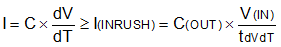
The inrush current is determined as shown in Equation 8.

Equation 8. GUID-50B6F12B-8875-4CFC-9C91-BC9026C71F2B-low.gif

Average power dissipated during start-up is given by Equation 9.

Equation 9. GUID-BACAC4EB-243D-48F8-8863-4784FBB1FE93-low.gif

Equation 9 assumes that the load does not draw any current until the output voltage reaches its final value.