ZHCSI22F October 2017 – December 2021 TPS2662
PRODUCTION DATA
- 1 特性
- 2 应用
- 3 说明
- 4 Revision History
- 5 Device Comparison Table
- 6 Pin Configuration and Functions
- 7 Specifications
- 8 Parameter Measurement Information
-
9 Detailed Description
- 9.1 Overview
- 9.2 Functional Block Diagram
- 9.3
Feature Description
- 9.3.1 Undervoltage Lockout (UVLO)
- 9.3.2 Overvoltage Protection (OVP)
- 9.3.3 Hot Plug-In and Inrush Current Control
- 9.3.4 Reverse Polarity Protection
- 9.3.5 Overload and Short-Circuit Protection
- 9.3.6 Reverse Current Protection
- 9.3.7 FAULT Response
- 9.3.8 IN, OUT, RTN, and GND Pins
- 9.3.9 Thermal Shutdown
- 9.4 Device Functional Modes
-
10Application and Implementation
- 10.1 Application Information
- 10.2 Typical Application
- 10.3 System Examples
- 10.4 Do's and Don'ts
- 11Power Supply Recommendations
- 12Layout
- 13Device and Documentation Support
- 14Mechanical, Packaging, and Orderable Information
9.3.5.2 Short-Circuit Protection
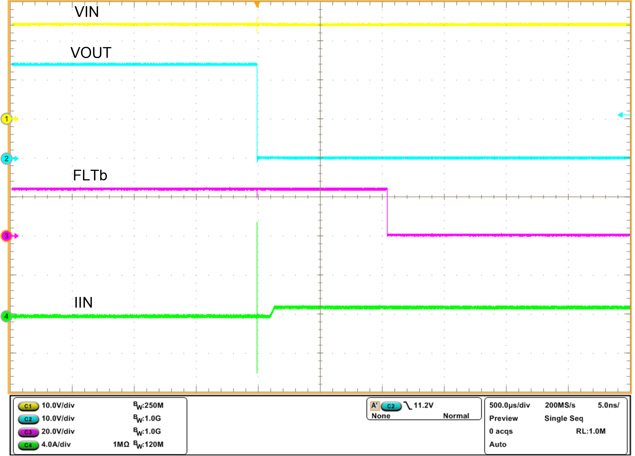
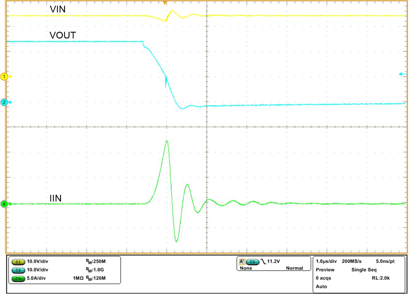
During a transient output short circuit event, the current through the device increases rapidly. As the current-limit amplifier cannot respond quickly to this event due to its limited bandwidth, the device incorporates a fast-trip comparator. The fast-trip comparator architecture is designed for fast turn OFF (tFAST-TRIP(dly) = 220 ns (typical)) of the internal FET during an output short circuit event. The fast-trip threshold is internally set to I(FAST-TRIP). The fast-trip circuit holds the internal FET off for only a few microseconds, after which the device turns back on slowly, allowing the current-limit loop to regulate the output current to I(OL). Then the device functions similar to the overload condition. Figure 9-10 and Figure 9-11 illustrate the behavior of the system during output short-circuit condition.

| VIN = 24 V, RILIM = 7.5 kΩ | ||
 Figure 9-11 Hot-Short: Fast-Trip Response (Zoomed)
The fast-trip comparator architecture has a supply line noise immunity resulting in a robust performance in noisy environments. This feature is achieved by controlling the turn OFF time of the internal FET based on the differential voltage across V(IN) and V(OUT) after the current through the device exceeds I(FAST-TRIP). Higher the voltage difference V(IN) – V(OUT), faster the turn OFF time, tFAST-TRIP(dly).