ZHCSI22F October 2017 – December 2021 TPS2662
PRODUCTION DATA
- 1 特性
- 2 应用
- 3 说明
- 4 Revision History
- 5 Device Comparison Table
- 6 Pin Configuration and Functions
- 7 Specifications
- 8 Parameter Measurement Information
-
9 Detailed Description
- 9.1 Overview
- 9.2 Functional Block Diagram
- 9.3
Feature Description
- 9.3.1 Undervoltage Lockout (UVLO)
- 9.3.2 Overvoltage Protection (OVP)
- 9.3.3 Hot Plug-In and Inrush Current Control
- 9.3.4 Reverse Polarity Protection
- 9.3.5 Overload and Short-Circuit Protection
- 9.3.6 Reverse Current Protection
- 9.3.7 FAULT Response
- 9.3.8 IN, OUT, RTN, and GND Pins
- 9.3.9 Thermal Shutdown
- 9.4 Device Functional Modes
-
10Application and Implementation
- 10.1 Application Information
- 10.2 Typical Application
- 10.3 System Examples
- 10.4 Do's and Don'ts
- 11Power Supply Recommendations
- 12Layout
- 13Device and Documentation Support
- 14Mechanical, Packaging, and Orderable Information
9.3.6 Reverse Current Protection
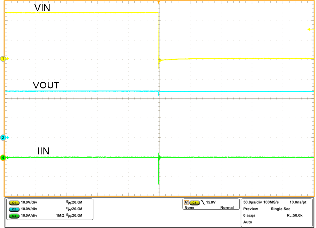
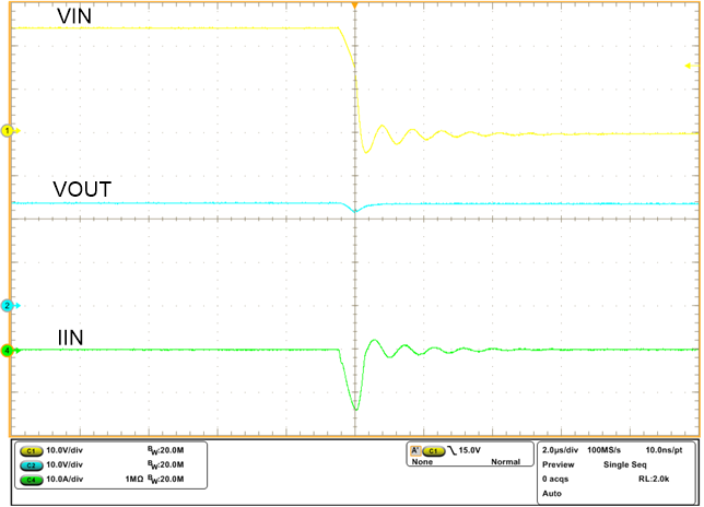
The device monitors V(IN) and V(OUT) to provide true reverse current blocking when a reverse condition or input power failure condition is detected. The reverse comparator turns OFF the internal FET within 310 ns (typical) as soon as V(IN) – V(OUT) falls below –2.6 V. The reverse comparator turns on within 63 µs (typical) after the differential forward voltage V(IN)– V(OUT) exceeds 115 mV. Figure 9-13 and Figure 9-14 illustrate the behavior of the system during input hot short circuit condition.
 Figure 9-13 Input Hot Short Functionality at 24-V Supply
 Figure 9-14 Hot-Short: Fast-Trip
Response (Zoomed)
Figure 9-14 Hot-Short: Fast-Trip
Response (Zoomed)The reverse comparator architecture has a supply line noise immunity resulting in a robust performance in noisy environments. This feature is achieved by controlling the turn OFF time of the internal FET based on the over-drive differential voltage V(IN) – V(OUT) over V(REVTH). Higher the over-drive, faster the turn OFF time, tREV(dly). Figure 7-22 shows the reverse current blocking response time versus over-drive voltage.