ZHCSCK8G May 2014 – October 2017 LP8860-Q1
PRODUCTION DATA.
- 1 特性
- 2 应用
- 3 说明
- 4 修订历史记录
- 5 器件比较表
- 6 Pin Configuration and Functions
-
7 Specifications
- 7.1 Absolute Maximum Ratings
- 7.2 ESD Ratings
- 7.3 Recommended Operating Conditions
- 7.4 Thermal Information
- 7.5 Electrical Characteristics
- 7.6 Current Sinks Electrical Characteristics
- 7.7 Boost Converter Characteristics
- 7.8 Logic Interface Characteristics
- 7.9 VIN Undervoltage Protection (VIN_UVLO)
- 7.10 VDD Undervoltage Protection (VDD_UVLO)
- 7.11 VIN Overvoltage Protection (VIN_OVP)
- 7.12 VIN Overcurrent Protection (VIN_OCP)
- 7.13 Power-Line FET Control Electrical Characteristics
- 7.14 External Temp Sensor Control Electrical Characteristics
- 7.15 I2C Serial Bus Timing Parameters (SDA, SCLK)
- 7.16 SPI Timing Requirements
- 7.17 Typical Characteristics
-
8 Detailed Description
- 8.1 Overview
- 8.2 Functional Block Diagram
- 8.3 Feature Description
- 8.4 Device Functional Modes
- 8.5 Programming
- 8.6
Register Maps
- 8.6.1
Register Bit Explanations
- 8.6.1.1 Display/Cluster1 Brightness Control MSB
- 8.6.1.2 Display/Cluster1 Brightness Control LSB
- 8.6.1.3 Display/Cluster1 Output Current MSB
- 8.6.1.4 Display/Cluster1 Output Current LSB
- 8.6.1.5 Cluster2 Brightness Control MSB
- 8.6.1.6 Cluster2 Brightness Control LSB
- 8.6.1.7 Cluster2 Output Current
- 8.6.1.8 Cluster3 Brightness Control MSB
- 8.6.1.9 Cluster3 Brightness Control LSB
- 8.6.1.10 Cluster3 Output Current
- 8.6.1.11 Cluster4 Brightness Control MSB
- 8.6.1.12 Cluster4 Brightness Control LSB
- 8.6.1.13 Cluster4 Output Current
- 8.6.1.14 Configuration
- 8.6.1.15 Status
- 8.6.1.16 Fault
- 8.6.1.17 LED Fault
- 8.6.1.18 Fault Clear
- 8.6.1.19 Identification
- 8.6.1.20 Temp MSB
- 8.6.1.21 Temp LSB
- 8.6.1.22 Display LED Current MSB
- 8.6.1.23 Display LED Current LSB
- 8.6.1.24 Display LED PWM MSB
- 8.6.1.25 Display LED PWM LSB
- 8.6.1.26 EEPROM Control
- 8.6.1.27 EEPROM Unlock Code
- 8.6.2
EEPROM Bit Explanations
- 8.6.2.1 EEPROM Register 0
- 8.6.2.2 EEPROM Register 1
- 8.6.2.3 EEPROM Register 2
- 8.6.2.4 EEPROM Register 3
- 8.6.2.5 EEPROM Register 4
- 8.6.2.6 EEPROM Register 5
- 8.6.2.7 EEPROM Register 6
- 8.6.2.8 EEPROM Register 7
- 8.6.2.9 EEPROM Register 8
- 8.6.2.10 EEPROM Register 9
- 8.6.2.11 EEPROM Register 10
- 8.6.2.12 EEPROM Register 11
- 8.6.2.13 EEPROM Register 12
- 8.6.2.14 EEPROM Register 13
- 8.6.2.15 EEPROM Register 14
- 8.6.2.16 EEPROM Register 15
- 8.6.2.17 EEPROM Register 16
- 8.6.2.18 EEPROM Register 17
- 8.6.2.19 EEPROM Register 18
- 8.6.2.20 EEPROM Register 19
- 8.6.2.21 EEPROM Register 20
- 8.6.2.22 EEPROM Register 21
- 8.6.2.23 EEPROM Register 22
- 8.6.2.24 EEPROM Register 23
- 8.6.2.25 EEPROM Register 24
- 8.6.1
Register Bit Explanations
-
9 Application and Implementation
- 9.1 Application Information
- 9.2
Typical Applications
- 9.2.1
Typical Application for Display Backlight
- 9.2.1.1 Design Requirements
- 9.2.1.2
Detailed Design Procedure
- 9.2.1.2.1 Inductor Selection
- 9.2.1.2.2 Output Capacitor Selection
- 9.2.1.2.3 Input Capacitor Selection
- 9.2.1.2.4 Charge Pump Output Capacitor
- 9.2.1.2.5 Charge Pump Flying Capacitor
- 9.2.1.2.6 Diode
- 9.2.1.2.7 Boost Converter Transistor
- 9.2.1.2.8 Boost Sense Resistor
- 9.2.1.2.9 Power Line Transistor
- 9.2.1.2.10 Input Current Sense Resistor
- 9.2.1.2.11 Filter Component Values
- 9.2.1.3 Application Performance Plots
- 9.2.2 Low VDD Voltage and Combined Output Mode Application
- 9.2.3 High Output Voltage Application
- 9.2.4 High Output Current Application
- 9.2.5 Three-Channel Configuration Without Serial Interface
- 9.2.6 Solution With Minimum External Components
- 9.2.1
Typical Application for Display Backlight
- 10Power Supply Recommendations
- 11Layout
- 12器件和文档支持
- 13机械、封装和可订购信息
8.3.9.5 Protection Feature and Fault Summary
Table 17 summarizes protection features and related faults.
Table 17. Overview of the Fault/Protection Schemes
| FAULT/PROTECTION | FAULT NAME | THRESHOLD | ACTION(1)(2) | MASK(4) | FAULT CLEARING(3)(5) | |
|---|---|---|---|---|---|---|
| Input overvoltage protection | VIN_OVP | OVP_LEVEL[1:0] (V) | VIN overvoltage monitored from soft start. Fault causes entry to FAULT_RECOVERY state. If device is restarted successfully with recovery timer, the fault register bit is not automatically cleared.
FAULT pin is pulled low. |
MASK_OVP_FSM
Masks fault recovery, but not status and fault pin operations |
Fault bit and FAULT pin:
1. POR or VDDIO/EN 2. Writing CLEAR_FAULTS bit or toggling NSS pin |
|
| 00 | OFF | |||||
| 01 | 7 | |||||
| 10 | 11 | |||||
| 11 | 22.5 | |||||
| Input undervoltage protection | VIN_UVLO | UVLO_LEVEL[1:0] (V) | VIN undervoltage monitored from soft start. Fault causes entry to FAULT_RECOVERY state. If device is restarted successfully with recovery timer, the fault register bit is not automatically cleared.
FAULT pin is pulled low. |
MASK_VIN_UVLO
Masks fault recovery, status and fault pin operations |
Fault bit and FAULT pin:
1.POR or VDDIO/EN 2. Writing CLEAR_FAULTS bit or toggling NSS pin |
|
| 00 | OFF | |||||
| 01 | 3 | |||||
| 10 | 5 | |||||
| 11 | 8 | |||||
| VDD undervoltage protection | VDD_UVLO | VDD_UVLO_LEVEL
Threshold (V) |
Device enters STANDBY state. Recovers when fault disappears. All registers are cleared or reloaded from EEPROM (if defined) with exception registers 0x00, 0x01, 0x04…0x0C. After recovery LP8860-Q1 provides the same brightness as before fault detection, if DISP_CL1_CURRENT[11:0] context stays same as LED_CURRENT_CTRL[11:0] EEPROM setting. If VDD voltage goes below POR level, registers 0x00, 0x01, 0x04…0x0C are cleared.
This fault does not have any flags and doesn’t generate FAULT. Voltage hysteresis is 50 mV (typical). |
|||
| 0 | 2.5 | |||||
| 1 | 3 | |||||
| Boost overcurrent protection | BOOST_OCP | VBOOST longer than 110 ms 5 V (typical) below set value.
Set value is voltage value defined by logic during adaptation in adaptive mode or initial boost voltage setting in manual mode. |
Fault monitoring started from boost start. Fault causes entry to FAULT_RECOVERY state. If device is restarted successfully with recovery timer, the fault register bit is not automatically cleared.
FAULT pin is pulled low. |
MASK_BOOST_OCP_ FSM
Masks fault recovery, but not status and fault pin operations |
Fault bit and FAULT pin:
1. POR or VDDIO/EN 2. Writing CLEAR_FAULTS bit or toggling NSS pin |
|
| Boost overvoltage protection | BOOST_OVP | VBOOST voltage 1.6 V (typical) above set value
Set value is voltage value defined by logic during adaptation in adaptive mode or initial boost voltage setting in manual mode. |
Boost OVP fault monitored during normal operation
FAULT pin is pulled low. |
MASK_BOOST_OVP_ STATUS | Fault bit and FAULT pin:
1. POR or VDDIO/EN 2. Writing CLEAR_FAULTS bit or toggling NSS pin |
|
| Input voltage overcurrent protection | PL_FET_FAULT | PL_SD_LEVEL[1:0] (A) | Fault is detected with 2 methods:
1. Detects overcurrent from soft start by measuring RISENSE voltage. 2. Detects FB voltage at the end of soft start. If voltage is below 1.2 V, fault is detected. Fault causes entry to FAULT_RECOVERY state. If device is restarted successfully with recovery timer, the fault register bit is not automatically cleared. FAULT pin is pulled low. |
Fault bit and FAULT pin:
1. POR or VDDIO/EN 2. Writing CLEAR_FAULTS bit or toggling NSS pin |
||
| 10 | 6 | |||||
| 11 | 8 | |||||
| Short LED fault | SHORT_LED | DRV_LED_FAULT_THR[1:0] (V) | LED output in display mode: Triggered if one or more outputs voltage is above DRV_LED_FAULT_THR and at least one LED output voltage is between DRV_HEADR and DRV_HEADR + DRV_LED_COMP_HYST. Is set only if LED faults are enabled in EEPROM. Shorted string is removed from voltage control loop and LED current sink n is disabled.
LED output in cluster mode: If one or more outputs voltage above DRV_LED_FAULT_THR fault is detected. Is pulled low only if LED faults are enabled in EEPROM. Shorted string PWM output is disabled. FAULT pin is pulled low. |
EN_DISPLAY_LED_ FAULT for LEDs in display mode EN_CL_LED_FAULT for LEDs in cluster mode | Fault bit and FAULT pin:
1. POR or VDDIO/EN 2. Writing CLEAR_FAULTS bit or toggling NSS pin When fault is cleared it can be set again only during next POR or if there is another LED short fault in different output. |
|
| 00 | 3.6 | |||||
| 01 | 3.6 | |||||
| 10 | 6.9 | |||||
| 11 | 10.6 | |||||
| DRV_LED_COMP_HYST[1:0] (mV) | ||||||
| 00 | 1000 | |||||
| 01 | 750 | |||||
| 10 | 500 | |||||
| 11 | 250 | |||||
| Open LED fault | OPEN_LED | DRV_HEADR[2:0] (mV) | LED output in display mode: Triggered if one or more outputs voltage is below DRV_HEADR, and boost adaptive control has reach the maximum voltage. Is set only if led faults enabled in EEPROM. Open string is removed from voltage control loop and PWM generation is disabled.
LED output in cluster mode: Triggered if one or more outputs voltage is below DRV_HEADR. Is set only if LED faults enabled in EEPROM. Open string PWM generation is disabled. FAULT pin is pulled low. |
EN_DISPLAY_LED
_FAULT for LEDs in display mode EN_CL_LED_FAULT for LEDs in cluster mode |
Fault bit and FAULT pin:
1. POR or VDDIO/EN 2. Writing CLEAR_FAULTS bit or toggling NSS pin When open fault is cleared it can set again only during next power-up or if there is another LED open fault. |
|
| 111 | VSAT+50 | |||||
| 110 | VSAT+175 | |||||
| 101 | VSAT+300 | |||||
| 100 | VSAT+450 | |||||
| 011 | VSAT+575 | |||||
| 010 | VSAT+700 | |||||
| 001 | VSAT+875 | |||||
| 000 | VSAT+1000 | |||||
| LED faults | LED_FAULT[4:1] | Defines which string has either open or short fault. Cleared only during power down. | POR or VDDIO/EN | |||
| Charge pump fault | CP_2X_ FAULT | VCPUMD< 0.85 × (2 × VDD) (typical) | Charge pump voltage not high enough condition. Fault causes entry to FAULT_RECOVERY state. CP voltage monitored from the boost soft start. If device is restarted successfully with recovery timer, the fault register bit is not automatically cleared.
FAULT pin is pulled low. |
Fault bit and FAULT pin:
1. POR or VDDIO/EN 2. Writing CLEAR_FAULTS bit or toggling NSS pin |
||
| Thermal Current Limit (LED Outputs) | No faults | INT_TEMP_LIM[1:0] | When die temperature increases temperature defined by INT_TEMP_LIM[1:0] the device automatically lowers the PWM duty for outputs 2.25%/ºC (typical). For Hybrid PWM and Current dimming mode current is used for brightness reduction as well. | |||
| 00
01 10 11 |
disabled
90°C 100°C 110°C |
|||||
| Thermal LED Current Limit with external NTC sensor. | EXT_TEMP_ FLAG_L | EXT_TEMP_LEVEL_LOW[3:0] | Fault is monitored during normal operation. If EXT_TEMP_LEVEL_LOW[3:0] is exceeded, LED current is reduced.
FAULT pin is pulled low when EXT_TEMP_FLAG_L goes high. |
EXT_TEMP_COMP_EN=0 disables fault | Fault bit:
1. POR or VDDIO/EN 2. Writing CLEAR_FAULTS bit or toggling NSS pin when fault deasserted. Fault pin: 1. POR or VDDIO/EN 2. Writing CLEAR_FAULTS bit or toggling NSS pin |
|
| Setting | Level (kΩ) | |||||
| 0000
0001 0010 0011 0100 0101 0110 0111 1000 1001 1010 1011 1100 1101 1110 1111 |
79.67
43.35 29.77 22.67 18.30 15.34 13.21 11.60 10.34 9.32 8.49 7.79 7.20 6.69 6.25 5.87 |
|||||
| EXT_TEMP_ FLAG_H | EXT_TEMP_LEVEL_HIGH[3:0] | Fault is monitored during normal operation. If EXT_TEMP_LEVEL_HIGH[3:0] limit is exceeded, the LED outputs are turned off.
FAULT pin is pulled low. |
EXT_TEMP_COMP_EN=0 disables fault | Fault bit:
1. POR or VDDIO/EN 2. Writing CLEAR_FAULTS bit or toggling NSS pin when fault deasserted. Fault pin: 1. POR or VDDIO/EN 2. Writing CLEAR_FAULTS bit or toggling NSS pin |
||
| Setting | Level (kΩ) | |||||
| 0000
0001 0010 0011 0100 0101 0110 0111 1000 1001 1010 1011 1100 1101 1110 1111 |
79.67
43.35 29.77 22.67 18.30 15.34 13.21 11.60 10.34 9.32 8.49 7.79 7.20 6.69 6.25 5.87 |
|||||
| NTC missing | TEMP_RES_ MISSING | Resistance > 2 MΩ | NTC is missing. Fault is monitored during normal operation. Not connected to FAULT output pin. TEMP_RES_FAULT is monitored if EXT_TEMP_COMP_EN EEPROM bit has been enabled | EXT_TEMP_COMP_EN=0 disables fault | 1. POR or VDDIO/EN
2. Writing CLEAR_FAULTS bit or toggling NSS pin |
|
| Thermal shutdown | TSD | Rising temperature =165ºC
Falling temperature = 135ºC |
Thermal shutdown is monitored from soft start. Fault causes entry to the FAULT_RECOVERY state.
FAULT pin is pulled low. |
Fault bit and FAULT pin:
1. POR or VDDIO/EN 2. Writing CLEAR_FAULTS bit or toggling NSS pin |
||
(1) Recovery time is 100 ms.
(2) During fault recovery state the LED outputs and boost is shut down and power-line FET is turned off.
(3) If fault is cleared during fault recovery state, FAULT pin is pulled low again after recovery state, if this fault still exists.
(4) If fault recovery is masked, fault bit sets again after cleaning.
(5) The NSS pin can be used for fault reset only for I2C interface mode. NSS is level sensitive; be aware NSS is set to low after fault reset.
Fault detection is digitally filtered — filtering time for different faults is shown in Table 18.
Table 18. Fault Filters
| FAULT/PROTECTON | FAULT NAME | TIME | ENABLED |
|---|---|---|---|
| Boost Overcurrent Protection | BOOST_OCP | 110 ms | From boost start |
| Boost Overvoltage Protection | BOOST_OVP | 100 µs | In normal mode |
| Input Overvoltage Protection | VIN_OVP | 100 µs | From soft start |
| Input Undervoltage Protection | VIN_UVLO | 100 µs | From soft start |
| Input Overcurrent Protection | PL_FET_FAULT | 100 µs | From soft start |
| VDD Undervoltage Protection | VDD_UVLO | 5 µs | Always |
| Thermal Shutdown | TSD | 100 µs | From soft start |
| Charge Pump fault | CP_2X_FAULT | 10 µs | From boost start |
| Thermal LED Current Limit with external NTC sensor. | EXT_TEMP_FLAG_H | 10 µs | In normal mode |
| EXT_TEMP_FLAG_L | 10 µs | In normal mode | |
| NTC missing | TEMP_RES_FAULT | 100 µs | In normal mode |
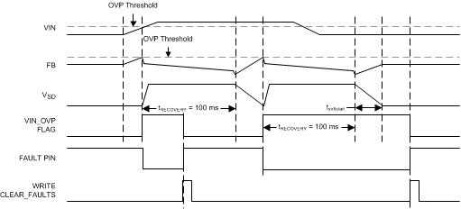 Figure 37. Input OVP Triggering and Recovery
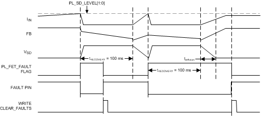 Figure 39. Input OVP Triggering and Recovery
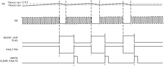 Figure 41. Boost OVP Triggering and Recovery
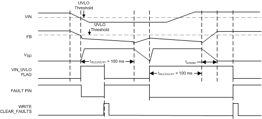 Figure 38. Input UVLO Triggering and Recovery
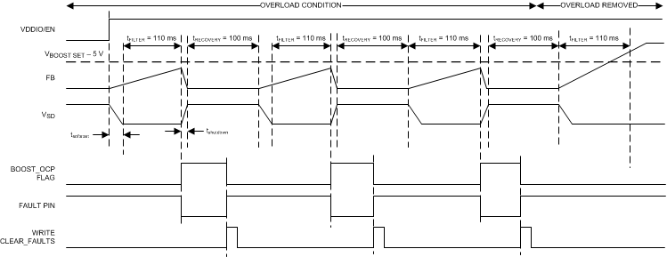 Figure 40. Boost OCP Triggering and Recovery