ZHCSIR1C June 2018 – May 2021 LM2775-Q1
PRODUCTION DATA
- 1 特性
- 2 应用
- 3 说明
- 4 Revision History
- 5 Pin Configuration and Functions
- 6 Specifications
- 7 Detailed Description
- 8 Application and Implementation
- 9 Power Supply Recommendations
- 10Layout
- 11Device and Documentation Support
- 12Mechanical, Packaging, and Orderable Information
8.2.2.1 Output Current Capability
The LM2775-Q1 provides 200 mA of output current when the input voltage is within 3.1 V to 5.5 V.
Understanding relevant application issues is recommended and a thorough analysis of the application circuit should be performed when using the part outside operating ratings and/or specifications to ensure satisfactory circuit performance in the application. Special care should be paid to power dissipation and thermal effects. These parameters can have a dramatic impact on high-current applications, especially when the input voltage is high. (see the Section 8.2.2.3 section).
The schematic of Figure 8-2 is a simplified model of the LM2775-Q1 that is useful for evaluating output current capability. The model shows a linear pre-regulation block (Reg), a voltage doubler (2×), and an output resistance (ROUT). Output resistance models the output voltage droop that is inherent to switched capacitor converters. The output resistance of the device is 3.5 Ω (typical) and is approximately equal to twice the resistance of the four LM2775-Q1 switches. When the output voltage is in regulation, the regulator in the model controls the voltage V' to keep the output voltage equal to 5 V ± 4%. With increased output current, the voltage drop across ROUT increases. To prevent droop in output voltage, the voltage drop across the regulator is reduced, V' increases, and VOUT remains at 5 V. When the output current increases to the point that there is zero voltage drop across the regulator, V' equals the input voltage, and the output voltage is near the edge of regulation. Additional output current causes the output voltage to fall out of regulation, and the LM2775-Q1 operation is similar to a basic open-loop doubler. As in a voltage doubler, increase in output current results in output voltage drop proportional to the output resistance of the doubler. The out-of-regulation LM2775-Q1 output voltage can be approximated by:
Again, Equation 1 only applies at low input voltage and high output current where the LM2775-Q1 is not regulating. See Output Current vs. Output Voltage curves in the Section 6.7 section for more details.
 Figure 8-2 LM2775-Q1 Output Resistance Model
A more complete calculation of output resistance takes into account the effects of switching frequency, flying capacitance, and capacitor equivalent series resistance (ESR) (see Equation 2).
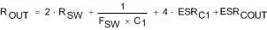
Switch resistance component (3 Ω typical) dominates the output resistance equation of the LM2775-Q1. With a 2-MHz typical switching frequency, the 1/(F×C) component of the output resistance contributes only 0.5 Ω to the total output resistance. Increasing the flying capacitance only provides minimal improvement to the total output current capability of the LM2775-Q1. In some applications it may be desirable to reduce the value of the flying capacitor below 1 µF to reduce solution size and/or cost, but this should be done with care so that output resistance does not increase to the point that undesired output voltage droop results. If ceramic capacitors are used, ESR will be a negligible factor in the total output resistance, as the ESR of quality ceramic capacitors is typically much less than 100 mΩ.