ZHCSIR1C June   2018  – May 2021 LM2775-Q1

PRODUCTION DATA  

  1. 特性
  2. 应用
  3. 说明
  4. Revision History
  5. Pin Configuration and Functions
  6. Specifications
    1. 6.1 Absolute Maximum Ratings
    2. 6.2 ESD Ratings
    3. 6.3 Recommended Operating Conditions
    4. 6.4 Thermal Information
    5. 6.5 Electrical Characteristics
    6. 6.6 Switching Characteristics
    7. 6.7 Typical Characteristics
  7. Detailed Description
    1. 7.1 Overview
    2. 7.2 Functional Block Diagram
    3. 7.3 Feature Description
      1. 7.3.1 Pre-Regulation
      2. 7.3.2 Input Current Limit
      3. 7.3.3 PFM Mode
      4. 7.3.4 Output Discharge
      5. 7.3.5 Thermal Shutdown
      6. 7.3.6 Undervoltage Lockout
    4. 7.4 Device Functional Modes
      1. 7.4.1 Shutdown
      2. 7.4.2 Boost Mode
  8. Application and Implementation
    1. 8.1 Application Information
    2. 8.2 Typical Application
      1. 8.2.1 Design Requirements
      2. 8.2.2 Detailed Design Procedure
        1. 8.2.2.1 Output Current Capability
        2. 8.2.2.2 Efficiency
        3. 8.2.2.3 Power Dissipation
        4. 8.2.2.4 Recommended Capacitor Types
        5. 8.2.2.5 Output Capacitor and Output Voltage Ripple
        6. 8.2.2.6 Input Capacitor and Input Voltage Ripple
        7. 8.2.2.7 Flying Capacitor
      3. 8.2.3 Application Curve
      4. 8.2.4 USB OTG / Mobile HDMI Power Supply
        1. 8.2.4.1 Design Requirements
        2. 8.2.4.2 Detailed Design Procedure
        3. 8.2.4.3 Application Curve
  9. Power Supply Recommendations
  10. 10Layout
    1. 10.1 Layout Guidelines
    2. 10.2 Layout Example
  11. 11Device and Documentation Support
    1. 11.1 接收文档更新通知
    2. 11.2 支持资源
    3. 11.3 Trademarks
    4. 11.4 Electrostatic Discharge Caution
    5. 11.5 Glossary
  12. 12Mechanical, Packaging, and Orderable Information

封装选项

机械数据 (封装 | 引脚)
散热焊盘机械数据 (封装 | 引脚)
订购信息

Pin Configuration and Functions

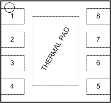
GUID-7874012C-8EA6-416E-90A1-580BE559C9AD-low.gif Figure 5-1 8-Pin WSON with Thermal PadDSG Package(Top View)
Table 5-1 Pin Functions
PIN I/O DESCRIPTION
NO. NAME
1 PFM I PFM mode enable. Allow or disallow PFM operation. 1 = PFM enabled, 0 = PFM disabled
2 C1– P Flying capacitor pin
3 C1+ P Flying capacitor pin
4 OUTDIS I Output disconnect option. 1 = Active output discharge during shutdown, 0 = High impedance output without pull-down during shutdown.
5 EN I Chip enable. 1 = Enabled, 0 = Disabled
6 VOUT O Charge pump output
7 VIN P Input voltage
8 GND G Ground
Thermal Pad GND GND Connect to GND