ZHCSIR1C June   2018  – May 2021 LM2775-Q1

PRODUCTION DATA  

  1. 特性
  2. 应用
  3. 说明
  4. Revision History
  5. Pin Configuration and Functions
  6. Specifications
    1. 6.1 Absolute Maximum Ratings
    2. 6.2 ESD Ratings
    3. 6.3 Recommended Operating Conditions
    4. 6.4 Thermal Information
    5. 6.5 Electrical Characteristics
    6. 6.6 Switching Characteristics
    7. 6.7 Typical Characteristics
  7. Detailed Description
    1. 7.1 Overview
    2. 7.2 Functional Block Diagram
    3. 7.3 Feature Description
      1. 7.3.1 Pre-Regulation
      2. 7.3.2 Input Current Limit
      3. 7.3.3 PFM Mode
      4. 7.3.4 Output Discharge
      5. 7.3.5 Thermal Shutdown
      6. 7.3.6 Undervoltage Lockout
    4. 7.4 Device Functional Modes
      1. 7.4.1 Shutdown
      2. 7.4.2 Boost Mode
  8. Application and Implementation
    1. 8.1 Application Information
    2. 8.2 Typical Application
      1. 8.2.1 Design Requirements
      2. 8.2.2 Detailed Design Procedure
        1. 8.2.2.1 Output Current Capability
        2. 8.2.2.2 Efficiency
        3. 8.2.2.3 Power Dissipation
        4. 8.2.2.4 Recommended Capacitor Types
        5. 8.2.2.5 Output Capacitor and Output Voltage Ripple
        6. 8.2.2.6 Input Capacitor and Input Voltage Ripple
        7. 8.2.2.7 Flying Capacitor
      3. 8.2.3 Application Curve
      4. 8.2.4 USB OTG / Mobile HDMI Power Supply
        1. 8.2.4.1 Design Requirements
        2. 8.2.4.2 Detailed Design Procedure
        3. 8.2.4.3 Application Curve
  9. Power Supply Recommendations
  10. 10Layout
    1. 10.1 Layout Guidelines
    2. 10.2 Layout Example
  11. 11Device and Documentation Support
    1. 11.1 接收文档更新通知
    2. 11.2 支持资源
    3. 11.3 Trademarks
    4. 11.4 Electrostatic Discharge Caution
    5. 11.5 Glossary
  12. 12Mechanical, Packaging, and Orderable Information

封装选项

机械数据 (封装 | 引脚)
散热焊盘机械数据 (封装 | 引脚)
订购信息

Typical Characteristics

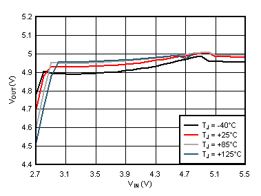
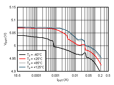
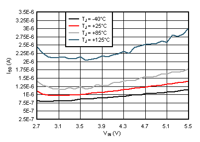
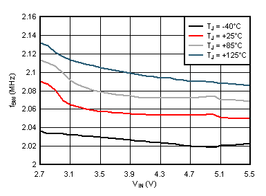
TJ = 25°C, VIN = 3.6 V, CIN = COUT = 10 µF (10-V 0402 case), C1 = 1 µF (10-V 0402 case), VEN = VIN.
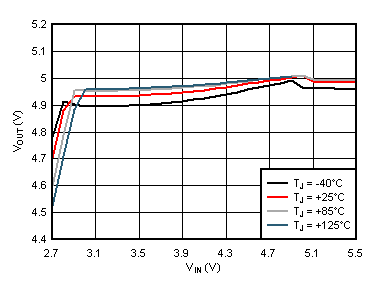
GUID-1EB85180-033E-4979-982B-11C492AC9457-low.gif
ILOAD = 200 mA PFM = '0'
Figure 6-1 PWM Output Regulation
GUID-AB08229F-34B3-4836-B3E7-373160150E4F-low.gif
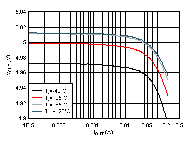
VIN = 3.3 V PFM = '0'
Figure 6-3 Load Regulation
GUID-7A54A56F-511F-486C-B7B3-CC81E3DAB686-low.gif
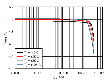
VIN = 2.7 V PFM = '0'
Figure 6-5 Load Regulation
GUID-5951EC06-6740-4D70-B764-9E347731EFB0-low.gif
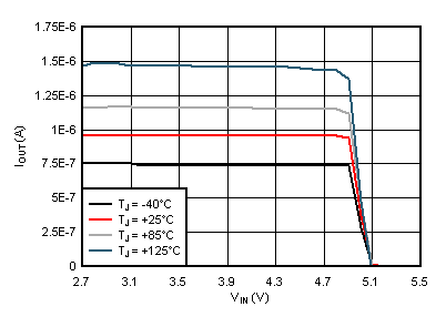
EN = '0' OUTDIS = '0'
Figure 6-7 Output Leakage Current
GUID-F1601D4B-A1C3-4442-A0D8-41AA6856CBD6-low.gif
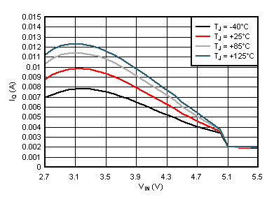
ILOAD = 0 mA PFM = '0'
Figure 6-9 PWM Quiescent Current
GUID-B2AAD33B-5285-43C1-9E3C-022B257D432B-low.gif
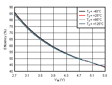
ILOAD = 100 mA PFM = '0'
Figure 6-11 Efficiency vs Input Voltage
GUID-CD987B37-EA57-4226-83AE-C6501F0CC7BD-low.gif
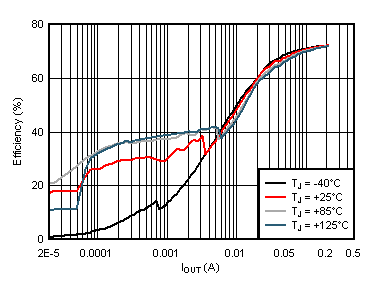
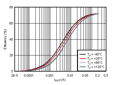
VIN = 3.3 V PFM = '1'
Figure 6-13 Efficiency vs Load Current
GUID-072F6195-5649-459D-8856-55C3B2F7E627-low.gif
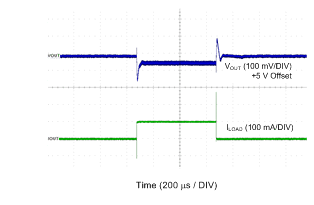
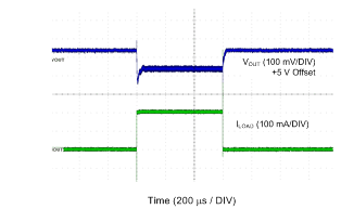
VIN = 3.6 V ILOAD = 1 mA to 100 mA PFM = '0'
Figure 6-15 PWM Load Step
GUID-35102A93-66E0-4738-B02E-129CE4918850-low.gif
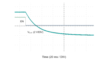
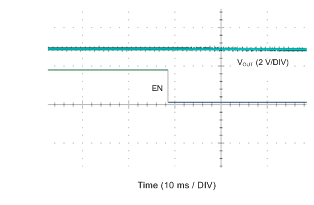
VIN = 3.6 V OUTDIS = '1'
Figure 6-17 Output Discharge Enabled
GUID-3E776AE1-A389-4597-94CF-904623F9519C-low.gif
ILOAD = 200 mA PFM = '1'
Figure 6-2 PFM Output Regulation
GUID-C1DFAF99-240F-4157-B4B4-21965D1E7F67-low.gif
VIN = 3.3 V PFM = '1'
Figure 6-4 Load Regulation
GUID-4B81C4DF-8280-4FD9-A42F-D30A7AF08E13-low.gif
EN = '0'
Figure 6-6 Shutdown Current
GUID-2F340394-7927-4AE4-A84E-CE668803317B-low.gif
ILOAD = 0 mA PFM = '1'
Figure 6-8 PFM Quiescent Current
GUID-B9B5058F-DCE9-4912-AFE8-428768676640-low.gifFigure 6-10 Switching Frequency
GUID-F7F33353-9383-4C35-970E-843F3FB35487-low.gif
VIN = 3.3 V PFM = '0'
Figure 6-12 Efficiency vs Load Current
GUID-5F08893A-8846-4644-9A75-6A7096417FEA-low.gif
VIN = 3.6 V ILOAD = 1 mA to 100 mA PFM = '1'
Figure 6-14 PFM Load Step
GUID-0C432F10-C16B-424F-B624-165FAF0E0632-low.gif
VIN = 3.6 V OUTDIS = '0'
Figure 6-16 Output Discharge Disabled
GUID-88147E87-9345-4929-B4FD-AC4E4F1DE810-low.gif
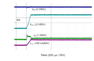
VIN = 3.6 V ILOAD = 100 mA
Figure 6-18 Start-Up into a Load