ZHCSD62F December 2012 – May 2021 LM25017
PRODUCTION DATA
- 1 特性
- 2 应用
- 3 说明
- 4 Revision History
- 5 Pin Configuration and Functions
- 6 Specifications
-
7 Detailed Description
- 7.1 Overview
- 7.2 Functional Block Diagram
- 7.3
Feature Description
- 7.3.1 Control Overview
- 7.3.2 VCC Regulator
- 7.3.3 Regulation Comparator
- 7.3.4 Overvoltage Comparator
- 7.3.5 On-Time Generator
- 7.3.6 Current Limit
- 7.3.7 N-Channel Buck Switch and Driver
- 7.3.8 Synchronous Rectifier
- 7.3.9 Undervoltage Detector
- 7.3.10 Thermal Protection
- 7.3.11 Ripple Configuration
- 7.3.12 Soft-Start
- 7.4 Device Functional Modes
-
8 Application and Implementation
- 8.1 Application Information
- 8.2
Typical Applications
- 8.2.1 Application Circuit: 12.5-V to 48-V Input and 10-V, 650-mA Output Buck Converter
- 8.2.2
Typical Isolated DC-DC Converter Using LM25017
- 8.2.2.1 Design Requirements
- 8.2.2.2
Detailed Design Procedure
- 8.2.2.2.1 Transformer Turns Ratio
- 8.2.2.2.2 Total IOUT
- 8.2.2.2.3 RFB1, RFB2
- 8.2.2.2.4 Frequency Selection
- 8.2.2.2.5 Transformer Selection
- 8.2.2.2.6 Primary Output Capacitor
- 8.2.2.2.7 Secondary Output Capacitor
- 8.2.2.2.8 Type III Feedback Ripple Circuit
- 8.2.2.2.9 Secondary Diode
- 8.2.2.2.10 VCC and Bootstrap Capacitor
- 8.2.2.2.11 Input Capacitor
- 8.2.2.2.12 UVLO Resistors
- 8.2.2.2.13 VCC Diode
- 8.2.2.3 Application Curves
- 9 Power Supply Recommendations
- 10Layout
- 11Device and Documentation Support
- 12Mechanical, Packaging, and Orderable Information
封装选项
机械数据 (封装 | 引脚)
散热焊盘机械数据 (封装 | 引脚)
- DDA|8
订购信息
8.2.2.2.6 Primary Output Capacitor
In a conventional buck converter the output ripple voltage is calculated as shown in Equation 24.

To limit the primary output ripple voltage ΔVOUT1 to approximately 25 mV, an output capacitor COUT1 of 0.9 µF would be required for a conventional buck.
Figure 8-6 shows the primary winding current waveform (IL1) of a Fly-Buck™ converter. The reflected secondary winding current adds to the primary winding current during the buck switch off-time. Because of this increased current, the output voltage ripple is not the same as in conventional buck converter. The output capacitor value calculated in Equation 24 should be used as the starting point. Optimization of output capacitance over the entire line and load range must be done experimentally. If the majority of the load current is drawn from the secondary isolated output, a better approximation of the primary output voltage ripple is given by Equation 25.
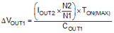
 Figure 8-6 Current Waveforms for COUT1 Ripple Calculation
To limit the primary output ripple voltage to approximately 100 mV, an output capacitor of 4 μF is required. A standard 4.7-µF, 16 V capacitor is selected for this design. If lower output voltage ripple is required, a higher value should be selected for COUT1 and/or COUT2.