ZHCSD62F December 2012 – May 2021 LM25017
PRODUCTION DATA
- 1 特性
- 2 应用
- 3 说明
- 4 Revision History
- 5 Pin Configuration and Functions
- 6 Specifications
-
7 Detailed Description
- 7.1 Overview
- 7.2 Functional Block Diagram
- 7.3
Feature Description
- 7.3.1 Control Overview
- 7.3.2 VCC Regulator
- 7.3.3 Regulation Comparator
- 7.3.4 Overvoltage Comparator
- 7.3.5 On-Time Generator
- 7.3.6 Current Limit
- 7.3.7 N-Channel Buck Switch and Driver
- 7.3.8 Synchronous Rectifier
- 7.3.9 Undervoltage Detector
- 7.3.10 Thermal Protection
- 7.3.11 Ripple Configuration
- 7.3.12 Soft-Start
- 7.4 Device Functional Modes
-
8 Application and Implementation
- 8.1 Application Information
- 8.2
Typical Applications
- 8.2.1 Application Circuit: 12.5-V to 48-V Input and 10-V, 650-mA Output Buck Converter
- 8.2.2
Typical Isolated DC-DC Converter Using LM25017
- 8.2.2.1 Design Requirements
- 8.2.2.2
Detailed Design Procedure
- 8.2.2.2.1 Transformer Turns Ratio
- 8.2.2.2.2 Total IOUT
- 8.2.2.2.3 RFB1, RFB2
- 8.2.2.2.4 Frequency Selection
- 8.2.2.2.5 Transformer Selection
- 8.2.2.2.6 Primary Output Capacitor
- 8.2.2.2.7 Secondary Output Capacitor
- 8.2.2.2.8 Type III Feedback Ripple Circuit
- 8.2.2.2.9 Secondary Diode
- 8.2.2.2.10 VCC and Bootstrap Capacitor
- 8.2.2.2.11 Input Capacitor
- 8.2.2.2.12 UVLO Resistors
- 8.2.2.2.13 VCC Diode
- 8.2.2.3 Application Curves
- 9 Power Supply Recommendations
- 10Layout
- 11Device and Documentation Support
- 12Mechanical, Packaging, and Orderable Information
封装选项
机械数据 (封装 | 引脚)
散热焊盘机械数据 (封装 | 引脚)
- DDA|8
订购信息
5 Pin Configuration and Functions
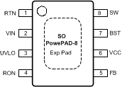
 Figure 5-1 8-Pin HSOPDDA PackageTop View
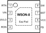
 Figure 5-2 8-Pin WSONNGU PackageTop View
Table 5-1 Pin Functions
| PIN | I/O | DESCRIPTION | APPLICATION INFORMATION | |
|---|---|---|---|---|
| NO. | NAME | |||
| 1 | RTN | — | Ground | Ground connection of the integrated circuit. |
| 2 | VIN | I | Input Voltage | Operating input range is 7.5 V to 48 V. |
| 3 | UVLO | I | Input Pin of Undervoltage Comparator | Resistor divider from VIN to UVLO to GND programs the undervoltage detection threshold. An internal current source is enabled when UVLO is above 1.225 V to provide hysteresis. When UVLO pin is pulled below 0.66 V externally, the regulator is in shutdown mode. |
| 4 | RON | I | On-Time Control | A resistor between this pin and VIN sets the buck switch on-time as a function of VIN. Minimum recommended on-time is 100 ns at max input voltage. |
| 5 | FB | I | Feedback | This pin is connected to the inverting input of the internal regulation comparator. The regulation level is 1.225 V. |
| 6 | VCC | O | Output from the Internal High Voltage Series Pass Regulator. Regulated at 7.6 V | The internal VCC regulator provides bias supply for the gate drivers and other internal circuitry. A 1.0-μF decoupling capacitor is recommended. |
| 7 | BST | I | Bootstrap Capacitor | An external capacitor is required between the BST and SW pins (0.01-μF ceramic). The BST pin capacitor is charged by the VCC regulator through an internal diode when the SW pin is low. |
| 8 | SW | O | Switching Node | Power switching node. Connect to the output inductor and bootstrap capacitor. |
| — | EP | — | Exposed Pad | Exposed pad must be connected to the RTN pin. Solder to the system ground plane on application board for reduced thermal resistance. |