ZHCSJ44D December 2018 – April 2022 INA819
PRODUCTION DATA
- 1 特性
- 2 应用
- 3 说明
- 4 Revision History
- 5 Device Comparison Table
- 6 Pin Configuration and Functions
- 7 Specifications
- 8 Detailed Description
- 9 Application and Implementation
- 10Power Supply Recommendations
- 11Layout
- 12Device and Documentation Support
- 13Mechanical, Packaging, and Orderable Information
封装选项
机械数据 (封装 | 引脚)
散热焊盘机械数据 (封装 | 引脚)
- DRG|8
订购信息
8.3.6 Error Sources
Most modern signal-conditioning systems calibrate errors at room temperature. However, calibration of errors that result from a change in temperature is normally difficult and costly. Therefore, minimize these errors by choosing high-precision components, such as the INA819, that have improved specifications in critical areas that impact the precision of the overall system. Figure 8-10 shows an example application.
 Figure 8-10 Example
Application with G = 10 V/V and 1-V Output Voltage
Figure 8-10 Example
Application with G = 10 V/V and 1-V Output VoltageResistor-adjustable devices (such as the INA819) show the lowest gain error in G = 1 because of the inherently well-matched drift of the internal resistors of the differential amplifier. At gains greater than 1 (for instance, G = 10 V/V or G = 100 V/V), the gain error becomes a significant error source because of the contribution of the resistor drift of the 25-kΩ feedback resistors in conjunction with the external gain resistor. Except for very high gain applications, the gain drift is by far the largest error contributor compared to other drift errors, such as offset drift.
The INA819 offers excellent gain error over temperature for both G > 1 and G = 1 (no external gain resistor). Table 8-4 summarizes the major error sources in common INA applications and compares the three cases of G = 1 (no external resistor) and G = 10 (5.49-kΩ external resistor) and G = 100 (511-Ω external resistor). All calculations are assuming an output voltage of VOUT = 1 V. Thus, the input signal VDIFF (given by VDIFF= VOUT/G) exhibits smaller and smaller amplitudes with increasing gain G. In this example, VDIFF = 1 mV at G = 1000. All calculations refer the error to the input for easy comparison and system evaluation. As Table 8-4 shows, errors generated by the input stage (such as input offset voltage) are more dominant at higher gain, while the effects of output stage are suppressed because they are divided by the gain when referring them back to the input. The gain error and gain drift error are much more significant for gains greater than 1 because of the contribution of the resistor drift of the 25-kΩ feedback resistors in conjunction with the external gain resistor. In most applications, static errors (absolute accuracy errors) can readily be removed during calibration in production, while the drift errors are the key factors limiting overall system performance.
| QUANTITY | VALUE | UNIT |
|---|---|---|
| VOUT | 1 | V |
| VCM | 10 | V |
| VS | 1 | V |
| RS+ | 1000 | Ω |
| RS– | 999 | Ω |
| RG tolerance | 0.01 | % |
| RG drift | 10 | ppm/°C |
| Temperature range upper limit | 105 | °C |
| ERROR SOURCE | ERROR CALCULATION | INA819 VALUES | ||||
|---|---|---|---|---|---|---|
| SPECIFICATION | UNIT | G = 1 ERROR (ppm) | G = 100 ERROR (ppm) | G = 1000 ERROR (ppm) | ||
| ABSOLUTE ACCURACY AT 25°C | ||||||
| Input offset voltage | VOSI / VDIFF | 35 | µV | 35 | 350 | 3500 |
| Output offset voltage | VOSO / (G × VDIFF) | 300 | µV | 300 | 300 | 300 |
| Input offset current | IOS × maximum (RS+, RS–) / VDIFF | 0.5 | nA | 1 | 5 | 50 |
| CMRR (min) | VCM / (10CMRR/20 × VDIFF) | 90 (G = 1), 110 (G = 10), 130 (G = 100) |
dB | 316 | 316 | 316 |
| PSRR (min) | (VCC – VS)/ (10PSRR/20 × VDIFF) | 110 (G = 1), 114 (G = 10), 130 (G = 100) |
dB | 3 | 20 | 32 |
| Gain error from INA (max) | GE(%) × 104 | 0.02 (G = 1), 0.15 (G = 10, 100) |
% | 200 | 1500 | 1500 |
| Gain error from external resistor RG (max) | GE(%) × 104 | 0.01 | % | 100 | 100 | 100 |
| Total absolute accuracy error (ppm) at 25°C, worst case | sum of all errors | — | — | 955 | 2591 | 5798 |
| Total absolute accuracy error (ppm) at 25°C, average | rms sum of all errors | — | — | 491 | 1604 | 3835 |
| DRIFT TO 105°C | ||||||
| Gain drift from INA (max) | GTC × (TA – 25) | 5 (G = 1), 35 (G = 10, 100) |
ppm/°C | 400 | 2800 | 2800 |
| Gain drift from external resistor RG (max) | GTC × (TA – 25) | 10 | ppm/°C | 800 | 800 | 800 |
| Input offset voltage drift (max) | (VOSI_TC / VDIFF) × (TA – 25) | 0.4 | µV/°C | 32 | 320 | 3200 |
| Output offset voltage drift | [VOSO_TC / ( G × VDIFF)] × (TA – 25) | 5 | µV/°C | 400 | 400 | 400 |
| Offset current drift | IOS_TC × maximum (RS+,
RS–) × (TA – 25) / VDIFF |
20 | pA/°C | 2 | 16 | 160 |
| Total drift error to 105°C (ppm), worst case | sum of all errors | — | — | 1634 | 4336 | 7360 |
| Total drift error to 105°C (ppm), typical | rms sum of all errors | — | — | 980 | 2957 | 4348 |
| RESOLUTION | ||||||
| Gain nonlinearity | 10 (G = 1, 10), 15 (G = 100) |
ppm of FS | 10 | 10 | 15 | |
| Voltage noise (at 1 kHz) | 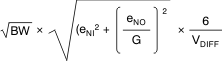 |
eNI = 8, eNO = 90 |
µVPP | 1204 | 1070 | 3941 |
| Current noise (at 1kHz) | IN × maximum (RS+, RS–) × √BW / VDIFF | 0.13 | pA/√ Hz | 0.3 | 2 | 11 |
| Total resolution error (ppm), worst case | sum of all errors | — | — | 1214 | 1080 | 3956 |
| Total resolution error (ppm), typical | rms sum of all errors | — | — | 1204 | 1070 | 3941 |
| TOTAL ERROR | ||||||
| Total error (ppm), worst case | sum of all errors | — | — | 3802 | 8007 | 17113 |
| Total error (ppm), typical | rms sum of all errors | — | — | 1628 | 3530 | 7010 |