ZHCSJ44D December 2018 – April 2022 INA819
PRODUCTION DATA
- 1 特性
- 2 应用
- 3 说明
- 4 Revision History
- 5 Device Comparison Table
- 6 Pin Configuration and Functions
- 7 Specifications
- 8 Detailed Description
- 9 Application and Implementation
- 10Power Supply Recommendations
- 11Layout
- 12Device and Documentation Support
- 13Mechanical, Packaging, and Orderable Information
封装选项
机械数据 (封装 | 引脚)
散热焊盘机械数据 (封装 | 引脚)
- DRG|8
订购信息
9.1.1 Reference Pin
The output voltage of the INA819 is developed with respect to the voltage on the reference pin (REF.) Often, in dual-supply operation, REF (pin 6) is connected to the low-impedance system ground. In single-supply operation, offsetting the output signal to a precise midsupply level is useful (for example, 2.5 V in a 5-V supply environment). To accomplish this level shift, a voltage source must be connected to the REF pin to level-shift the output so that the INA819 drives a single-supply analog-to-digital converter (ADC).
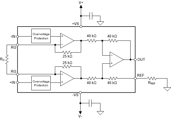
The voltage source applied to the reference pin must have a low output impedance. As shown in Figure 9-1, any resistance at the reference pin (shown as RREF in Figure 9-1) is in series with an internal 40-kΩ resistor.
 Figure 9-1 Parasitic Resistance Shown at the Reference Pin
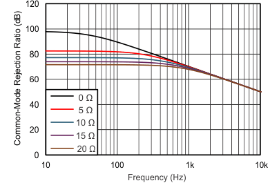
The parasitic resistance at the reference pin (RREF) creates an imbalance in the four resistors of the internal difference amplifier that results in a degraded common-mode rejection ratio (CMRR). Figure 9-2 shows the degradation in CMRR of the INA819 as a result of increased resistance at the reference pin. For the best performance, keep the source impedance to the REF pin (RREF) less than 5 Ω.
 Figure 9-2 The Effect of Increasing Resistance at the Reference Pin
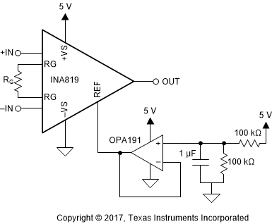
Voltage reference devices are an excellent option for providing a low-impedance voltage source for the reference pin. However, if a resistor voltage divider generates a reference voltage, the divider must be buffered by an op amp, as Figure 9-3 shows, to avoid CMRR degradation.
 Figure 9-3 Using an Op Amp to Buffer Reference Voltages