ZHCSJ44D December 2018 – April 2022 INA819
PRODUCTION DATA
- 1 特性
- 2 应用
- 3 说明
- 4 Revision History
- 5 Device Comparison Table
- 6 Pin Configuration and Functions
- 7 Specifications
- 8 Detailed Description
- 9 Application and Implementation
- 10Power Supply Recommendations
- 11Layout
- 12Device and Documentation Support
- 13Mechanical, Packaging, and Orderable Information
封装选项
机械数据 (封装 | 引脚)
散热焊盘机械数据 (封装 | 引脚)
订购信息
9.1.2 Input Bias Current Return Path
The input impedance of the INA819 is extremely high—approximately 100 GΩ. However, a path must be provided for the input bias current of both inputs. This input bias current is typically 150 pA. High input impedance means that this input bias current changes very little with varying input voltage.
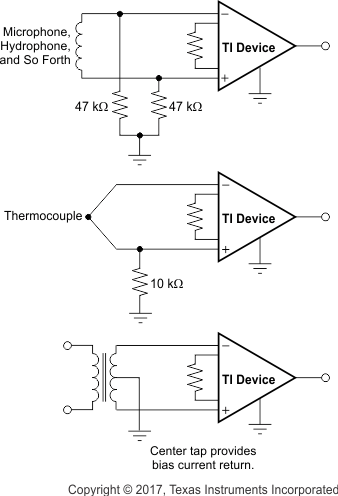
For proper operation, input circuitry must provide a path for input bias current. Figure 9-4 shows various provisions for an input bias current path. Without a bias current path, the inputs float to a potential that exceeds the common-mode range of the INA819, and the input amplifiers saturate. If the differential source resistance is low, the bias current return path can connect to one input (as shown in the thermocouple example in Figure 9-4). With a higher source impedance, using two equal resistors provides a balanced input with possible advantages of a lower input offset voltage as a result of bias current and better high-frequency common-mode rejection.
 Figure 9-4 Providing an Input Common-Mode Current Path