ZHCSJ44D December 2018 – April 2022 INA819
PRODUCTION DATA
- 1 特性
- 2 应用
- 3 说明
- 4 Revision History
- 5 Device Comparison Table
- 6 Pin Configuration and Functions
- 7 Specifications
- 8 Detailed Description
- 9 Application and Implementation
- 10Power Supply Recommendations
- 11Layout
- 12Device and Documentation Support
- 13Mechanical, Packaging, and Orderable Information
封装选项
机械数据 (封装 | 引脚)
散热焊盘机械数据 (封装 | 引脚)
- DRG|8
订购信息
9.2.1.2 Detailed Design Procedure
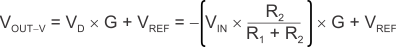
There are two modes of operation for the circuit shown in Figure 9-5: current input and voltage input. This design requires R1 >> R2 >> R3. Given this relationship, Equation 3 calculates the current input mode transfer function.

where
- G represents the gain of the instrumentation amplifier.
- VD represents the differential voltage at the INA819 inputs.
- VREF is the voltage at the INA819 REF pin.
- IIN is the input current.
Equation 4 shows the transfer function for the voltage input mode.
where
- VIN is the input voltage.
R1 sets the input impedance of the voltage input mode. The minimum typical input impedance is 100 kΩ. The R1 value is 100 kΩ because increasing the R1 value also increases noise. The value of R3 must be extremely small compared to R1 and R2. 20 Ω for R3 is selected because that resistance value is much smaller than R1 and yields an input voltage of ±400 mV when operated in current mode (±20 mA).
Use Equation 5 to calculate R2 given VD = ±400 mV, VIN = ±10 V, and R1 = 100 kΩ.
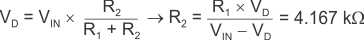
The value obtained from Equation 5 is not a standard 0.1% value, so 4.17 kΩ is selected. R1 and R2 also use 0.1% tolerance resistors to minimize error.
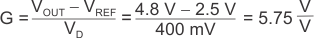
Use Equation 6 to calculate the ideal gain of the instrumentation amplifier.
Equation 7 calculates the gain-setting resistor value using the INA819 gain equation (Equation 1).
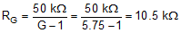
Use a standard 0.1% resistor value of 10.5 kΩ for this design.