ZHCSDE7A February   2015  – March 2021 INA225-Q1

PRODUCTION DATA  

  1. 特性
  2. 应用
  3. 说明
  4. Revision History
  5. Pin Configuration and Functions
  6. Specifications
    1. 6.1 Absolute Maximum Ratings (1)
    2. 6.2 ESD Ratings
    3. 6.3 Recommended Operating Conditions
    4. 6.4 Thermal Information
    5. 6.5 Electrical Characteristics
    6. 6.6 Typical Characteristics
  7. Detailed Description
    1. 7.1 Overview
    2. 7.2 Functional Block Diagram
    3. 7.3 Feature Description
      1. 7.3.1 Selecting A Shunt Resistor
        1. 7.3.1.1 Selecting A Current-Sense Resistor Example
        2. 7.3.1.2 Optimizing Power Dissipation versus Measurement Accuracy
      2. 7.3.2 Programmable Gain Select
    4. 7.4 Device Functional Modes
      1. 7.4.1 Input Filtering
      2. 7.4.2 Shutting Down the Device
      3. 7.4.3 Using the Device with Common-Mode Transients Above 36 V
  8. Applications and Implementation
    1. 8.1 Application Information
    2. 8.2 Typical Applications
      1. 8.2.1 Microcontroller-Configured Gain Selection
        1. 8.2.1.1 Design Requirements
        2. 8.2.1.2 Detailed Design Procedure
        3. 8.2.1.3 Application Curve
      2. 8.2.2 Unidirectional Operation
        1. 8.2.2.1 Design Requirements
        2. 8.2.2.2 Detailed Design Procedure
        3. 8.2.2.3 Application Curve
      3. 8.2.3 Bidirectional Operation
        1. 8.2.3.1 Design Requirements
        2. 8.2.3.2 Detailed Design Procedure
        3. 8.2.3.3 Application Curve
  9. Power Supply Recommendations
  10. 10Layout
    1. 10.1 Layout Guidelines
    2. 10.2 Layout Example
  11. 11Device and Documentation Support
    1. 11.1 Documentation Support
      1. 11.1.1 Related Documentation
    2. 11.2 接收文档更新通知
    3. 11.3 支持资源
    4. 11.4 Trademarks
    5. 11.5 静电放电警告
    6. 11.6 术语表
  12. 12Mechanical, Packaging, and Orderable Information

封装选项

机械数据 (封装 | 引脚)
散热焊盘机械数据 (封装 | 引脚)
订购信息

Pin Configuration and Functions

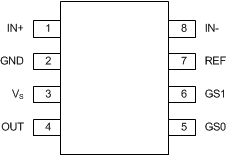
GUID-9CF4A854-B4CB-4CA1-8A5F-2674212349E4-low.gif Figure 5-1 DGK PackageVSSOP-8(Top View)
Table 5-1 Pin Functions
PIN I/O DESCRIPTION
NO. NAME
1 IN+ Analog input Connect to supply side of shunt resistor.
2 GND Analog Ground
3 VS Analog Power supply, 2.7 V to 36 V
4 OUT Analog output Output voltage
5 GS0 Digital input Gain select. Connect to VS or GND.
Table 7-3 lists terminal settings and the corresponding gain value.
6 GS1 Digital input Gain select. Connect to VS or GND.
Table 7-3 lists terminal settings and the corresponding gain value.
7 REF Analog input Reference voltage, 0 V to VS
8 IN– Analog input Connect to load side of shunt resistor.