ZHCSDE7A February 2015 – March 2021 INA225-Q1
PRODUCTION DATA
- 1 特性
- 2 应用
- 3 说明
- 4 Revision History
- 5 Pin Configuration and Functions
- 6 Specifications
- 7 Detailed Description
- 8 Applications and Implementation
- 9 Power Supply Recommendations
- 10Layout
- 11Device and Documentation Support
- 12Mechanical, Packaging, and Orderable Information
7.4.1 Input Filtering
An obvious and straightforward location for filtering is at the device output; however, this location negates the advantage of the low output impedance of the internal buffer. The input then represents the best location for implementing external filtering. Figure 7-1 shows the typical implementation of the input filter for the device.
 Figure 7-1 Input Filter
Care must be taken in the selection of the external filter component values because these components can affect device measurement accuracy. Placing external resistance in series with the input terminals creates an additional error so these resistors should be kept as low of a value as possible with a recommended maximum value of
10 Ω or less. Increasing the value of the input filter resistance beyond 10 Ω results in a smaller voltage signal present at the device input terminals than what is developed across the current-sense shunt resistor.
The internal bias network shown in Figure 7-1 creates a mismatch in the two input bias current paths when a differential voltage is applied between the input terminals. Under normal conditions, where no external resistance is added to the input paths, this mismatch of input bias currents has little effect on device operation or accuracy. However, when additional external resistance is added (such as for input filtering), the mismatch of input bias currents creates unequal voltage drops across these external components. The mismatched voltages result in a signal reaching the input terminals that is lower in value than the signal developed directly across the current-sensing resistor.
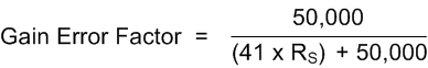
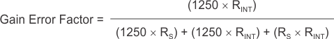
The amount of variance in the differential voltage present at the device input relative to the voltage developed at the shunt resistor is based both on the external series resistance value (RS) and the internal input resistors (RINT = 25 kΩ). The reduction of the shunt voltage reaching the device input terminals appears as a gain error when comparing the output voltage relative to the voltage across the shunt resistor. A factor can be calculated to determine the amount of gain error that is introduced by the addition of external series resistance.
The amount of error these external filter resistors introduce into the measurement can be calculated using the simplified gain error factor in Equation 1, where the gain error factor is calculated with Equation 2.
where:
- RINT is the internal input impedance, and
- RS is the external series resistance.
For example, using the gain error factor (Equation 1), a 10-Ω series resistance results in a gain error factor of 0.992. The corresponding gain error is then calculated using Equation 3, resulting in a gain error of approximately 0.81% solely because of the external 10-Ω series resistors. Using 100-Ω filter resistors increases this gain error to approximately 7.58% from these resistors alone.
