SLVSNH6 November 2026 DP83TC1104-Q1
PRODUCTION DATA
- 1
- 1 Features
- 2 Applications
- 3 Description
- 4 Device Comparison Table
- 5 Pin Configuration and Functions
- 6 Specifications
-
7 Detailed Description
- 7.1 Overview
- 7.2 Functional Block Diagram
- 7.3
Feature Description
- 7.3.1 MAC Security Features
- 7.3.2 IEEE802.1AS Features
- 7.3.3
TC10 Sleep Wake-up
- 7.3.3.1 Functions of the PHY for TC10 Support
- 7.3.3.2 Power Supply Networks for Sleep Applications
- 7.3.3.3 Configuration for Non-TC10 Applications
- 7.3.3.4 Miscellaneous Sleep Features
- 7.3.3.5 Fast Wake-up
- 7.3.4 PPM Monitor
- 7.3.5 Clock Dithering
- 7.3.6
Diagnostic Toolkit
- 7.3.6.1 Signal Quality Indicator
- 7.3.6.2 Electrostatic Discharge Sensing
- 7.3.6.3 Time Domain Reflectometry
- 7.3.6.4 BIST and Loopback Modes
- 7.3.7 Compliance Test Modes
- 7.4 Device Functional Modes
- 7.5 Output Slew Control
- 7.6 Programming
- 8 Register Maps
- 9 Application and Implementation
- 10Device and Documentation Support
- 11Revision History
- 12Mechanical, Packaging, and Orderable Information
9.3 Power Supply Recommendations
The DP83TC1104x-Q1 requires VDDA (core analog voltage), VDDIO (IO supply voltage) and VSLEEP (always-on supply for sleep). A 3.3V external power supply must be connected to VDDA through a decoupling network and an optional ferrite bead. The recommended power supply de-coupling network is shown in the figure below.
The DP83TC1104x-Q1 can operate with a wide range of IO supply voltages (3.3V, 2.5V, or 1.8V). No power supply sequencing is required. The recommended power supply de-coupling network is shown in the figure below. For improved conducted emissions, an optional ferrite bead can be placed between the supply and the PHY de-coupling network.
Typical TC-10 application block diagram along with supply and peripherals is shown below. TPS7B81-Q1 is the recommended part number to be used as 3.3V LDO for the VSLEEP rail. The low quiescent current of this LDO makes it appropriate for TC-10 applications. Some example power distribution networks for TC10 applications are explained in the TC10 sections of this datasheet.
VDD1P0 is fed from an LDO internal to DP83TC1104x-Q1. Connect decoupling network of 2.2uF and 0.1uF to VDD1P0 (Pin 3). An external supply must not be connected to VDD1P0.
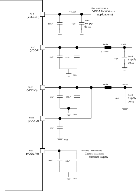 Figure 9-6 Power Supply Decoupling Network -
DP83TC1104x-Q1