SLVSNH6 November 2026 DP83TC1104-Q1
PRODUCTION DATA
- 1
- 1 Features
- 2 Applications
- 3 Description
- 4 Device Comparison Table
- 5 Pin Configuration and Functions
- 6 Specifications
-
7 Detailed Description
- 7.1 Overview
- 7.2 Functional Block Diagram
- 7.3
Feature Description
- 7.3.1 MAC Security Features
- 7.3.2 IEEE802.1AS Features
- 7.3.3
TC10 Sleep Wake-up
- 7.3.3.1 Functions of the PHY for TC10 Support
- 7.3.3.2 Power Supply Networks for Sleep Applications
- 7.3.3.3 Configuration for Non-TC10 Applications
- 7.3.3.4 Miscellaneous Sleep Features
- 7.3.3.5 Fast Wake-up
- 7.3.4 PPM Monitor
- 7.3.5 Clock Dithering
- 7.3.6
Diagnostic Toolkit
- 7.3.6.1 Signal Quality Indicator
- 7.3.6.2 Electrostatic Discharge Sensing
- 7.3.6.3 Time Domain Reflectometry
- 7.3.6.4 BIST and Loopback Modes
- 7.3.7 Compliance Test Modes
- 7.4 Device Functional Modes
- 7.5 Output Slew Control
- 7.6 Programming
- 8 Register Maps
- 9 Application and Implementation
- 10Device and Documentation Support
- 11Revision History
- 12Mechanical, Packaging, and Orderable Information
5 Pin Configuration and Functions
 Figure 5-1 DP83TC1104A-Q1 RHA
Package 36-Pin
VQFN
Top View
| PIN | TYPE(1) | DESCRIPTION | |
|---|---|---|---|
| NAME(2) | NO. | ||
| MAC INTERFACE | |||
|
RX_D3 |
20 | S, PD, O |
Receive Data: Symbols received on the cable are decoded and transmitted out of these pins synchronous to the rising edge of RX_CLK. They contain valid data when RX_DV is asserted. A data nibble, RX_D[3:0], is transmitted in MII and RGMII modes. 2 bits; RX_D[1:0], are transmitted in RMII mode. RX_D[3:2] are not used when in RMII Follower mode. If the PHY is bootstrapped to RMII Leader mode, a 50MHz clock reference is automatically outputted on RX_D3. This clock must be fed to the MAC. |
|
RX_D2 / STRAP_4 |
21 | ||
|
RX_D1 / STRAP_3 |
23 | ||
|
RX_D0 / STRAP_2 |
24 | ||
| RX_CLK / STRAP_6 | 26 | S, PD, O |
Receive Clock: In MII and RGMII modes, the receive clock provides a 25MHz reference clock. Unused in RMII mode |
| RX_ER / GPIO_0 / STRAP_1 | 19 | S, PD, O |
Receive Error: In MII and RMII modes, this pin indicates a receive error symbol has been detected within a received packet. In MII mode, RX_ER is asserted high synchronously to the rising edge of RX_CLK. In RMII mode, RX_ER is asserted high synchronously to the rising edge of the reference clock. This pin is optional in MII or RMII because the PHY will automatically corrupt data on a receive error. Unused in RGMII mode |
| RX_CTRL / RX_DV / CRS_DV / STRAP_0 | 25 | S, PD, O |
RGMII Receive Control: Receive control combines receive data valid indication and receive error indication into a single signal. RX_DV is presented on the rising edge of RX_CLK and RX_ER is presented on the falling edge of RX_CLK. Receive Data Valid: This pin indicates when valid data is presented on RX_D[3:0] for MII mode. Carrier Sense Data Valid: This pin combines carrier sense and data valid into an asynchronous signal. When CRS_DV is asserted, data is presented on RX_D[1:0] in RMII mode. |
| TX_CLK | 29 | PD, I, O |
Transmit Clock: In MII mode, the transmit clock is a 25MHz output (50Ω Driver). In RGMII mode, this clock is sourced from the MAC layer to the PHY. A 25MHz clock must be provided in RGMII mode to meet the RGMII timing requirements mentioned in section 6.6 Timing Requirements. Unused in RMII mode |
| TX_CTRL / TX_EN | 30 | PD, I |
RGMII Transmit Control: Transmit control combines transmit enable and transmit error indication into a single signal. TX_EN is presented before the rising edge of TX_CLK; TX_ER is presented before the falling edge of TX_CLK. Transmit Enable: In MII mode, transmit enable is presented before the rising edge of the transmit clock. TX_EN indicates the presence of valid data inputs on TX_D[3:0]. In RMII Follower mode, transmit enable is presented before the rising edge of the reference clock. In RMII Leader mode, transmit enable is presented before the rising edge of RX_D3. TX_EN indicates the presence of valid data inputs on TX_D[1:0]. |
| TX_D3 | 34 | PD, I |
Transmit Data: In MII and RGMII modes, the transmit data nibble, TX_D[3:0], is received from the MAC before the rising edge of TX_CLK. In RMII mode, TX_D[1:0] is received from the MAC before the rising edge of the reference clock. TX_D[3:2] are not used in RMII mode. |
| TX_D2 | 33 | ||
|
TX_D1 |
32 | ||
|
TX_D0 |
31 | ||
| SERIAL MANAGEMENT INTERFACE | |||
| MDC | 1 | I |
Management Data Clock: Synchronous clock to the MDIO serial management input and output data. This clock can be asynchronous to the MAC transmit and receive clocks. The maximum clock rate is 20MHz. There is no minimum clock rate. |
| MDIO | 36 | OD, IO |
Management Data Input/Output: Bidirectional management data signal that can be sourced by the management station or the PHY. This pin requires a pullup resistor. In systems with multiple PHYs using same MDIO-MDC bus, a single pull-up resistor to VDDIO must be used on MDIO line. Recommended to use a resistor from 2.2kΩ to 9kΩ. MDIO/MDC Access is required to pass Open Alliance Compliance. See Section 7.3.7. |
| CONTROL INTERFACE | |||
| INT | 2 | PU, OD, IO |
Interrupt: Active-LOW output, which is asserted LOW when an interrupt condition occurs. This pin has a weak internal pullup. Register access is necessary to enable various interrupt triggers. Once an interrupt event flag is set, register access is required to clear the interrupt event. This pin can be configured as an Active-HIGH output using register 0x0011. Interrupt status from Reg 12-13 is recommended to be read only when INT_N is LOW. This pin can also operate as Power-Down control where asserting this pin low would put the PHY in power down mode and asserting high would put the PHY in normal mode. This feature can also be enabled using register 0x0011. |
| RESET | 10 | PU, I |
Reset: Active-LOW input, which initializes or reinitializes the PHY. Asserting this pin LOW for at least 1μs forces a reset process to occur. All internal registers will reinitialize to the default states as specified for each bit in the Register Maps section. All bootstrap pins are resampled upon deassertion of reset. |
| WAKE | 11 |
PD, I/O |
WAKE: Input/Output pin which is Active-HIGH input by default. As input, this pin wakes the PHY from TC-10 SLEEP. Asserting this pin HIGH at power up brings the PHY out of SLEEP. External 10kΩ pull down resistor can be used when implementing TC-10 circuit to prevent accidental wake-up. This pin can be directly tied to VSLEEP or it can be pulled to VSLEEP using a resistor to wake the device. This pin also supports wake forwarding feature where a WAKE pulse generated by the PHY is then used to wake up other PHYs in the same system. |
| INH | 12 |
O, OD |
INH: Active-HIGH output. This pin is Hi-Z when the PHY is in TC-10 SLEEP. This pin is HIGH for all other PHY states. External pull down resistor in the range of 2kΩ - 10kΩ must be used when implementing TC-10 circuit. If multiple devices are sharing INH pin, then a single pulldown resistor must be used. |
| CLOCK INTERFACE | |||
| XI | 6 | I |
Reference Clock Input (RMII):Reference clock 50MHz CMOS-level oscillator in RMII Follower mode. Reference clock 25MHz crystal or oscillator in RMII Leader mode. Reference Clock Input (Other MAC Interfaces): Reference clock 25MHz crystal or oscillator input. The device supports either an external crystal resonator connected across pins XI and XO, or an external CMOS-level oscillator connected to pin XI only and XO left floating. This pin can also accept clock input from other devices like Ethernet MAC or another Ethernet PHY in daisy-chain operations. If using a crystal, connect a 100Ω resistor in series with the XI pin. |
| XO | 5 | O |
Reference Clock Output: XO pin is used for crystal only. This pin must be left floating when a CMOS-level oscillator is connected to XI. If using a crystal, connect a 100Ω resistor in series with the XO pin. |
| LED/GPIO INTERFACE | |||
| CLKOUT / GPIO_2 | 18 | S, PD, IO |
Clock Output: 25MHz reference clock. This pin can also be used as GPIO using register selection. |
| LED_1 / GPIO_1 / STRAP_5 | 17 | S, PD, IO |
LED_1: Link Status and BLINK for TX/RX Activity. This pin can also be used as GPIO using Strap/Register selection. |
| MEDIUM DEPENDENT INTERFACE | |||
| TRD_M | 15 | IO |
Differential Transmit and Receive: Bidirectional differential signaling configured for 100BASE-T1 operation, IEEE 802.3bw compliant. |
| TRD_P | 14 | ||
| POWER CONNECTIONS | |||
| VDDA | 7 | SUPPLY |
Core Supply: 3.3V Recommend using 0.47µF and 0.01µF ceramic decoupling capacitors; optional ferrite bead can be used. |
| VDDIO | 22, 35 | SUPPLY |
IO Supply: 1.8V, 2.5V, or 3.3V Recommend using ferrite bead, 0.47µF and 0.01µF ceramic decoupling capacitors on pin 22 and 0.01µF ceramic decoupling capacitors on pin 35. |
| VSLEEP | 9 | SUPPLY |
VSLEEP Supply: 3.3V Recommend using 0.1µF ceramic decoupling capacitors. |
| VDD1P0 | 3 | SUPPLY | VDD1P0 Supply Decoupling CAP External supply on Pin 3 is not supported. Recommend using 2.2-µF and 0.1µF ceramic decoupling capacitors. |
| GROUND | DAP | GROUND |
Ground: This must always be connected to power ground. |
| NO CONNECT | |||
| NC |
4, 8, 13, 16, 27, 28 |
NC: No connect (leave floating) |
|
I = Input
O = Output
IO = Input/Output
OD = Open Drain
PD = Internal pulldown
PU = Internal pullup
S = Bootstrap configuration pin (all configuration pins have weak internal pullups or pulldowns)
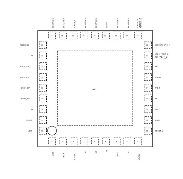 Figure 5-2 DP83TC1104B-Q1 RHA
Package 36-Pin
VQFN
Top View
| PIN | TYPE(1) | DESCRIPTION | |
|---|---|---|---|
| NAME(2) | NO. | ||
| MAC INTERFACE | |||
|
SGMII_SON |
30 | PD, O |
Receive Data: Symbols received on the cable are decoded and transmitted out of these pins. SGMII_SON / SOP are the positive and negative terminals of SGMII LVDS transmitter. When device is in RESET mode or if the supplies of the device are ramping up (before Power-On RESET), these pins must not be driven externally. |
|
SGMII_SOP |
31 | ||
|
SGMII_SIP |
32 | I |
Transmit Data: SGMII SIN / SIP are the positive and negative terminals of SGMII LVDS receiver. Data from the MAC is received on these pins, decoded and transmitted out on the MDI cable medium. |
|
SGMII_SIN |
33 | ||
| SERIAL MANAGEMENT INTERFACE | |||
| MDC | 1 | I |
Management Data Clock: Synchronous clock to the MDIO serial management input and output data. This clock can be asynchronous to the MAC transmit and receive clocks. The maximum clock rate is 20MHz. There is no minimum clock rate. |
| MDIO | 36 | OD, IO |
Management Data Input/Output: Bidirectional management data signal that can be sourced by the management station or the PHY. This pin requires a pullup resistor. In systems with multiple PHYs using same MDIO-MDC bus, a single pull-up resistor to VDDIO must be used on MDIO line. Recommended to use a resistor from 2.2kΩ to 9kΩ. MDIO/MDC Access is required to pass Open Alliance Compliance. See Section 7.3.7. |
| CONTROL INTERFACE | |||
| INT | 2 | PU, OD, IO |
Interrupt: Active-LOW output, which is asserted LOW when an interrupt condition occurs. This pin has a weak internal pullup. Register access is necessary to enable various interrupt triggers. Once an interrupt event flag is set, register access is required to clear the interrupt event. This pin can be configured as an Active-HIGH output using register 0x0011. Interrupt status from Reg 12-13 is recommended to be read only when INT_N is LOW. This pin can also operate as Power-Down control where asserting this pin low would put the PHY in power down mode and asserting high would put the PHY in normal mode. This feature can also be enabled using register 0x0011. |
| RESET | 10 | PU, I |
Reset: Active-LOW input, which initializes or reinitializes the PHY. Asserting this pin LOW for at least 1μs forces a reset process to occur. All internal registers will reinitialize to the default states as specified for each bit in the Register Maps section. All bootstrap pins are resampled upon deassertion of reset. |
| WAKE | 11 |
PD, I/O |
WAKE: Input/Output pin which is Active-HIGH input by default. As input, this pin wakes the PHY from TC-10 SLEEP. Asserting this pin HIGH at power up brings the PHY out of SLEEP. External 10kΩ pull down resistor can be used when implementing TC-10 circuit to prevent accidental wake-up. This pin can be directly tied to VSLEEP or it can be pulled to VSLEEP using a resistor to wake the device. This pin also supports wake forwarding feature where a WAKE pulse generated by the PHY is then used to wake up other PHYs in the same system. |
| INH | 12 |
O, OD |
INH: Active-HIGH output. This pin is Hi-Z when the PHY is in TC-10 SLEEP. This pin is HIGH for all other PHY states. External pull down resistor in the range of 2kΩ - 10kΩ must be used when implementing TC-10 circuit. If multiple devices are sharing INH pin, then a single pulldown resistor must be used. |
| CLOCK INTERFACE | |||
| XI | 6 | I |
Reference Clock Input: Reference clock 25MHz crystal or oscillator input. The device supports either an external crystal resonator connected across pins XI and XO, or an external CMOS-level oscillator connected to pin XI only and XO left floating. This pin can also accept clock input from other devices like Ethernet MAC or another Ethernet PHY in daisy-chain operations. If using a crystal, connect a 100Ω resistor in series with the XI pin. |
| XO | 5 | O |
Reference Clock Output: XO pin is used for crystal only. This pin must be left floating when a CMOS-level oscillator is connected to XI. If using a crystal, connect a 100Ω resistor in series with the XO pin. |
| LED/GPIO INTERFACE | |||
| CLKOUT / GPIO_2 | 18 | S, PD, IO |
Clock Output: 25MHz reference clock. This pin can also be used as GPIO using register selection. |
| LED_1 / GPIO_1 / STRAP_2 | 17 | S, PD, IO |
LED_1: Link Status and BLINK for TX/RX Activity. This pin can also be used as GPIO using Strap/Register selection. |
| MEDIUM DEPENDENT INTERFACE | |||
| TRD_M | 15 | IO |
Differential Transmit and Receive: Bidirectional differential signaling configured for 100BASE-T1 operation, IEEE 802.3bw compliant. |
| TRD_P | 14 | ||
| POWER CONNECTIONS | |||
| VDDA | 7 | SUPPLY |
Core Supply: 3.3V Recommend using 0.47µF and 0.01µF ceramic decoupling capacitors; optional ferrite bead can be used. |
| VDDIO | 22, 35 | SUPPLY |
IO Supply: 1.8V, 2.5V, or 3.3V Recommend using ferrite bead, 0.47µF and 0.01µF ceramic decoupling capacitors on pin 22 and 0.01µF ceramic decoupling capacitors on pin 35. |
| VSLEEP | 9 | SUPPLY |
VSLEEP Supply: 3.3V Recommend using 0.1µF ceramic decoupling capacitors. |
| VDD1P0 | 3 | SUPPLY | VDD1P0 Supply Decoupling CAP External supply on Pin 3 is not supported. Recommend using 2.2-µF and 0.1µF ceramic decoupling capacitors. |
| GROUND | DAP | GROUND |
Ground: This must always be connected to power ground. |
| NO CONNECT | |||
| NC |
4, 8, 13, 16, 27, 28 |
NC: No connect (leave floating) |
|
| STRAPS | |||
| STRAP_0 | 25 | S, PD | Strap Input: Used as PHY Address Strap |
| STRAP_1 / GPIO_0 | 19 | S, PD | Strap Input: Used as PHY Address Strap. This pin can also be used as GPIO through register selection. |
| RESERVED | |||
| RESERVED | 28 | I | RESERVED: Can be connected to a signal not exceeding VDDIO voltage. |
| RESERVED | 27 | I | RESERVED: Can be connected to VDDIO supply or a signal not exceeding VDDIO voltage. |
| RESERVED | 26 | I, PD | RESERVED: Can be connected to a signal not exceeding VDDIO voltage.
When device is in RESET mode or if the supplies of the device are ramping up (before Power-On RESET), this pin must not be driven externally. |
| RESERVED | 24 | I, PD |
RESERVED: Can be connected to a signal not exceeding VDDIO voltage. When device is in RESET mode or if the supplies of the device are ramping up (before Power-On RESET), this pin must not be driven externally. |
| RESERVED | 23 | I, PD | RESERVED: Can be connected to a signal not exceeding VDDIO voltage.
When device is in RESET mode or if the supplies of the device are ramping up (before Power-On RESET), this pin must not be driven externally. |
| RESERVED | 21 | I | RESERVED: Can be connected to a signal not exceeding VDDIO voltage. |
| RESERVED | 20 | I | RESERVED: Can be connected to a signal not exceeding VDDIO voltage. |