ZHCSI19F April 2010 – April 2018 DLPC200
PRODUCTION DATA.
- 1 特性
- 2 应用
- 3 说明
- 4 修订历史记录
- 5 Pin Configuration and Functions
-
6 Specifications
- 6.1 Absolute Maximum Ratings
- 6.2 Handling Ratings
- 6.3 Recommended Operating Conditions
- 6.4 Thermal Information
- 6.5 I/O Electrical Characteristics
- 6.6 Video Input Pixel Interface Timing Requirements
- 6.7 I2C Interface Timing Requirements
- 6.8 USB Read Interface Timing Requirements
- 6.9 USB Write Interface Timing Requirements
- 6.10 SPI Slave Interface Timing Requirements
- 6.11 Parallel Flash Interface Timing Requirements
- 6.12 Serial Flash Interface Timing Requirements
- 6.13 Static RAM Interface Timing Requirements
- 6.14 DMD Interface Timing Requirements
- 6.15 DLPA200 Interface Timing Requirements
- 6.16 DDR2 SDR Memory Interface Timing Requirements
- 6.17 Video Input Pixel Interface – Image Sync and Blanking Requirements
- 7 Detailed Description
-
8 Application and Implementation
- 8.1 Application Information
- 8.2
Typical Application
- 8.2.1 Design Requirements
- 8.2.2
Detailed Design Procedure
- 8.2.2.1
DLPC200 System Interfaces
- 8.2.2.1.1 DLPC200 Master, I2C Interface for EDID Programming
- 8.2.2.1.2 USB Interface
- 8.2.2.1.3 Bus Protocol
- 8.2.2.1.4 SPI Slave Interface
- 8.2.2.1.5 Parallel Flash Memory Interface
- 8.2.2.1.6 Serial Flash Memory Interface
- 8.2.2.1.7 SRAM Interface
- 8.2.2.1.8 DDR2 SDR Memory Interface
- 8.2.2.1.9 Projector Image and Control Port Signals
- 8.2.2.1.10 SDRAM Memory
- 8.2.2.1
DLPC200 System Interfaces
- 8.2.3 Application Curve
- 9 Power Supply Recommendations
- 10Layout
- 11器件和文档支持
- 12机械、封装和可订购信息
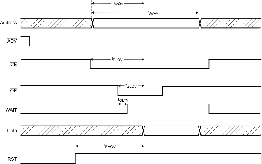
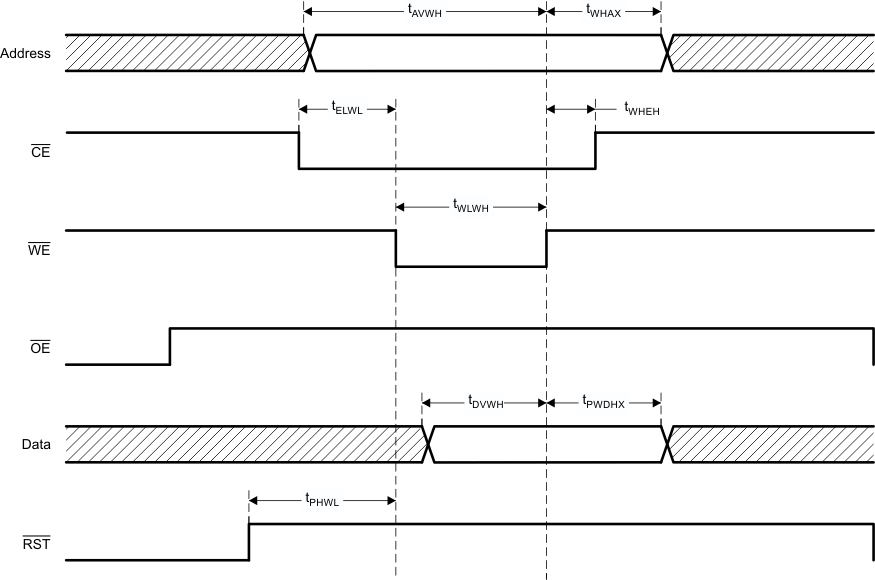
6.11 Parallel Flash Interface Timing Requirements
| PARAMETER | MIN | MAX | UNIT | |
|---|---|---|---|---|
| tAVAV | Read cycle time | 110 | ns | |
| tAVQV | Address to output valid | 110 | ns | |
| tELQV | CE low to output valid | 110 | ns | |
| tGLQV | OE low to output valid | 25 | ns | |
| tPHQV | RST high to output valid | 150 | ns | |
| tGLTV | OE low to WAIT valid | 17 | ns | |
| tPHWL | RST high recovery to WE low | 150 | ns | |
| tELWL | CE setup to WE low | 0 | ns | |
| tWLWH | WE write pulse width low | 50 | ns | |
| tDVWH | Data setup to WE high | 50 | ns | |
| tAVWH | Address setup to WE high | 50 | ns | |
| tWHEH | CE hold from WE high | 0 | ns | |
| tPWDHX | Data hold from WE high | 0 | ns | |
| tWHAX | Address hold from WE high | 0 | ns | |

