ZHCSI19F April 2010 – April 2018 DLPC200
PRODUCTION DATA.
- 1 特性
- 2 应用
- 3 说明
- 4 修订历史记录
- 5 Pin Configuration and Functions
-
6 Specifications
- 6.1 Absolute Maximum Ratings
- 6.2 Handling Ratings
- 6.3 Recommended Operating Conditions
- 6.4 Thermal Information
- 6.5 I/O Electrical Characteristics
- 6.6 Video Input Pixel Interface Timing Requirements
- 6.7 I2C Interface Timing Requirements
- 6.8 USB Read Interface Timing Requirements
- 6.9 USB Write Interface Timing Requirements
- 6.10 SPI Slave Interface Timing Requirements
- 6.11 Parallel Flash Interface Timing Requirements
- 6.12 Serial Flash Interface Timing Requirements
- 6.13 Static RAM Interface Timing Requirements
- 6.14 DMD Interface Timing Requirements
- 6.15 DLPA200 Interface Timing Requirements
- 6.16 DDR2 SDR Memory Interface Timing Requirements
- 6.17 Video Input Pixel Interface – Image Sync and Blanking Requirements
- 7 Detailed Description
-
8 Application and Implementation
- 8.1 Application Information
- 8.2
Typical Application
- 8.2.1 Design Requirements
- 8.2.2
Detailed Design Procedure
- 8.2.2.1
DLPC200 System Interfaces
- 8.2.2.1.1 DLPC200 Master, I2C Interface for EDID Programming
- 8.2.2.1.2 USB Interface
- 8.2.2.1.3 Bus Protocol
- 8.2.2.1.4 SPI Slave Interface
- 8.2.2.1.5 Parallel Flash Memory Interface
- 8.2.2.1.6 Serial Flash Memory Interface
- 8.2.2.1.7 SRAM Interface
- 8.2.2.1.8 DDR2 SDR Memory Interface
- 8.2.2.1.9 Projector Image and Control Port Signals
- 8.2.2.1.10 SDRAM Memory
- 8.2.2.1
DLPC200 System Interfaces
- 8.2.3 Application Curve
- 9 Power Supply Recommendations
- 10Layout
- 11器件和文档支持
- 12机械、封装和可订购信息
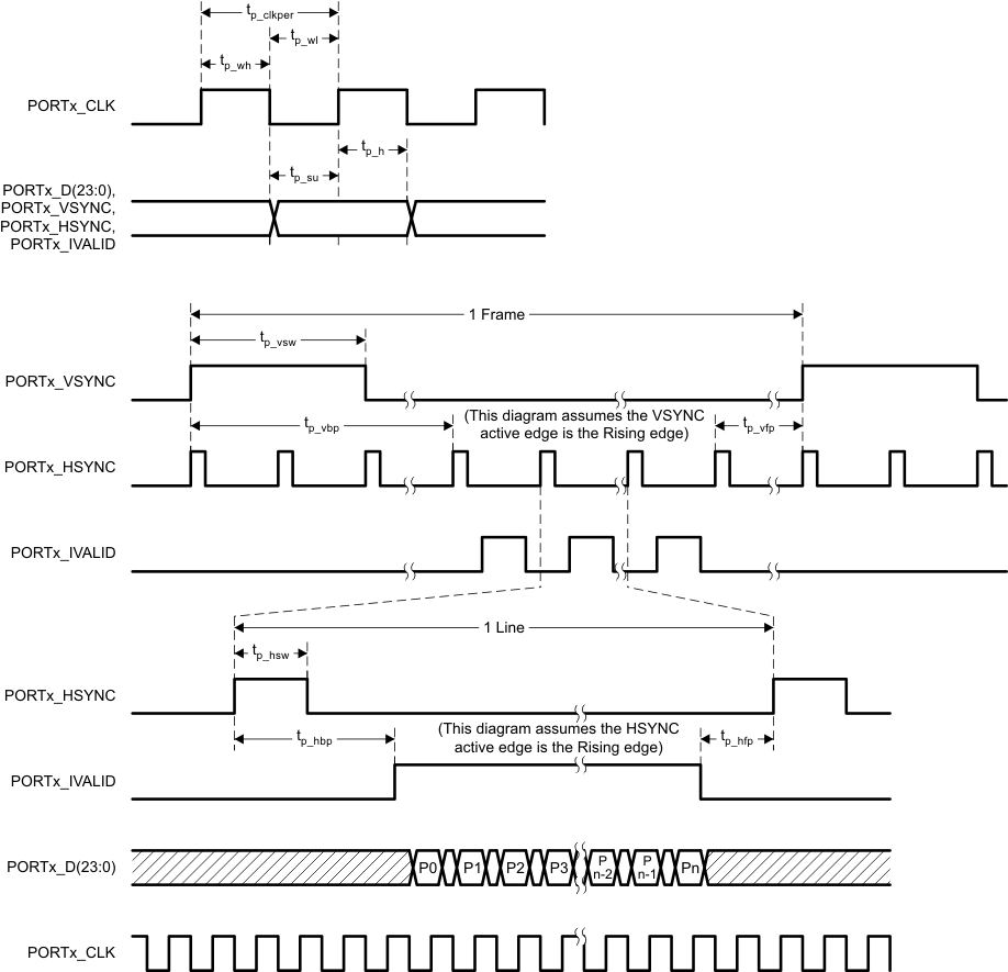
6.6 Video Input Pixel Interface Timing Requirements
| PARAMETER | TEST CONDITIONS | MIN | MAX | UNIT | |
|---|---|---|---|---|---|
| ƒpclock | Clock frequency, PORTx_CLK | 80 | MHz | ||
| tp_wh | Pulse duration, high | 45% to 55% reference points (signal) | 5.6 | ns | |
| tp_wl | Pulse duration, low | 45% to 55% reference points (signal) | 5.6 | ns | |
| tp_su | Setup time, PORTx_D(23–0) valid before PORTx_CLK | See (1) | 1.5 | ns | |
| tp_h | Hold time, PORTx_D(23–0) valid after PORTx_CLK | See (1) | 1.5 | ns | |
| tp_su | Setup time, PORTx_VSYNC valid before PORTx_CLK | See (1) | 1.5 | ns | |
| tp_h | Hold time, PORTx_VSYNC valid after PORTx_CLK | See (1) | 1.5 | ns | |
| tp_su | Setup time, PORTx_HSYNC valid before PORTx_CLK | See (1) | 1.5 | ns | |
| tp_h | Hold time, PORTx_HSYNC valid after PORTx_CLK | See (1) | 1.5 | ns | |
| tp_su | Setup time, PORTx_IVALID valid before PORTx_CLK | See (1) | 1.5 | ns | |
| tp_h | Hold time, PORTx_IVALID valid after PORTx_CLK | See (1) | 1.5 | ns | |
(1) PCLK may be inverted from that shown in Figure 1. In that case, the same specifications in the table are valid except now referenced to the falling edge of the clock. If the falling edge of PCLK is used, a USB or SPI command must be sent to tell the DLPC200 to use the falling edge of PCLK.
See Pin Configuration and Functions for the proper connection schema if a video input port will not be used.
