ZHCSE87A October   2015  – September 2023 DLPA3000

PRODUCTION DATA  

  1.   1
  2. 特性
  3. 应用
  4. 说明
  5. Revision History
  6. 说明(续)
  7. Pin Configuration and Functions
  8. Specifications
    1. 7.1 Absolute Maximum Ratings
    2. 7.2 ESD Ratings
    3. 7.3 Recommended Operating Conditions
    4. 7.4 Thermal Information
    5. 7.5 Electrical Characteristics
    6. 7.6 SPI Timing Parameters
  9. Detailed Description
    1. 8.1 Overview
    2. 8.2 功能方框图
    3. 8.3 Feature Description
      1. 8.3.1 Supply and Monitoring
        1. 8.3.1.1 Supply
        2. 8.3.1.2 Monitoring
          1. 8.3.1.2.1 Block Faults
          2. 8.3.1.2.2 Low Battery and UVLO
          3. 8.3.1.2.3 Auto LED Turn Off Functionality
          4. 8.3.1.2.4 Thermal Protection
      2. 8.3.2 Illumination
        1. 8.3.2.1 Programmable Gain Block
        2. 8.3.2.2 LDO Illum
        3. 8.3.2.3 Illumination Driver A
        4. 8.3.2.4 RGB Strobe Decoder
          1. 8.3.2.4.1 Break Before Make (BBM)
          2. 8.3.2.4.2 Openloop Voltage
          3. 8.3.2.4.3 Transient Current Limit
        5. 8.3.2.5 Illumination Monitoring
          1. 8.3.2.5.1 Power Good
          2. 8.3.2.5.2 Ratio Metric Overvoltage Protection
        6. 8.3.2.6 Load Current and Supply Voltage
        7. 8.3.2.7 Illumination Driver Plus Power FETS Efficiency
      3. 8.3.3 DMD Supplies
        1. 8.3.3.1 LDO DMD
        2. 8.3.3.2 DMD HV Regulator
          1. 8.3.3.2.1 Power-Up and Power-Down Timing
        3. 8.3.3.3 DMD/DLPC Buck Converters
        4. 8.3.3.4 DMD Monitoring
          1. 8.3.3.4.1 Power Good
          2. 8.3.3.4.2 Overvoltage Fault
      4. 8.3.4 Buck Converters
        1. 8.3.4.1 LDO Bucks
        2. 8.3.4.2 General Purpose Buck Converters
        3. 8.3.4.3 Buck Converter Monitoring
          1. 8.3.4.3.1 Power Good
          2. 8.3.4.3.2 Overvoltage Fault
        4. 8.3.4.4 Buck Converter Efficiency
      5. 8.3.5 Auxiliary LDOs
      6. 8.3.6 Measurement System
      7. 8.3.7 Digital Control
        1. 8.3.7.1 SPI
        2. 8.3.7.2 Interrupt
        3. 8.3.7.3 Fast-Shutdown in Case of Fault
    4. 8.4 Device Functional Modes
    5. 8.5 Register Maps
  10. Application and Implementation
    1. 9.1 Application Information
    2. 9.2 Typical Applications
      1. 9.2.1 Typical Application Setup Using DLPA3000
        1. 9.2.1.1 Design Requirements
        2. 9.2.1.2 Detailed Design Procedure
        3. 9.2.1.3 Application Curve
      2. 9.2.2 Typical Application with DLPA3000 Internal Block Diagram
  11. 10Power Supply Recommendations
  12. 11Layout
    1. 11.1 Layout Guidelines
    2. 11.2 Layout Example
    3. 11.3 SPI Connections
    4. 11.4 RLIM Routing
    5. 11.5 LED Connection
    6. 11.6 Thermal Considerations
  13. 12Device and Documentation Support
    1. 12.1 第三方产品免责声明
    2. 12.2 Device Support
      1. 12.2.1 Device Nomenclature
    3. 12.3 Related Links
    4. 12.4 接收文档更新通知
    5. 12.5 支持资源
    6. 12.6 Trademarks
    7. 12.7 支持资源
    8. 12.8 静电放电警告
    9. 12.9 术语表
  14. 13Mechanical, Packaging, and Orderable Information

封装选项

机械数据 (封装 | 引脚)
散热焊盘机械数据 (封装 | 引脚)
订购信息

RGB Strobe Decoder

The DLPA3000 contains circuitry to sequentially control the three color-LEDs (red, green and blue). This circuitry consists of three NMOS switches, the actual strobe decoder, and the LED current control (Figure 8-7). The NMOS switches are connected to the cathode terminals of the external LED package and turn on and off the currents through the LEDs.

GUID-6A8DA5BF-22A1-4BB2-9AD9-7099275C1306-low.gif Figure 8-7 Switch Connection for a Common-Anode LED assembly

The NMOS FETs P, Q, and R are controlled by the CH_SEL_0 and CH_SEL_1 pins. CH_SEL[1:0] typically receive a rotating code switching from RED to GREEN to BLUE and then back to RED. The relation between CH_SEL[0:1] and which switch is closed is indicated in Table 8-1.

Table 8-1 Switch Positions for Common Anode RGB LEDs
PINS CH_SEL[1:0] SWITCH IDAC REGISTER
P Q R
00 Open Open Open N/A
01 Closed Open Open SW1_IDAC[9:0]
10 Open Closed Open SW2_IDAC[9:0]
11 Open Open Closed SW3_IDAC[9:0]

Besides enabling one of the switches, CH_SEL[1:0] also selects a 10-bit current setting for the control IDAC that is used as the set current for the LED. This set current together with the measured current through RLIM is used to control the illumination driver to the appropriate VLED. The current through the 3 LEDs can be set independently by registers SW1_IDAC to SW3_IDAC, 0x03 to 0x08 (Table 8-1).

Each current level can be set from off to 150mV/RLIM in 1023 steps:

Equation 5. GUID-27992115-9AC6-4F14-BF5B-21AF0C85DF0F-low.gif

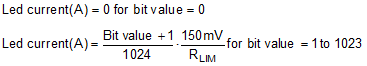
The maximum current for RLIM= 25 mΩ is thus 6 A.