ZHCSE87A October 2015 – September 2023 DLPA3000
PRODUCTION DATA
- 1
- 1 特性
- 2 应用
- 3 说明
- 4 Revision History
- 5 说明(续)
- 6 Pin Configuration and Functions
- 7 Specifications
-
8 Detailed Description
- 8.1 Overview
- 8.2 功能方框图
- 8.3
Feature Description
- 8.3.1 Supply and Monitoring
- 8.3.2 Illumination
- 8.3.3 DMD Supplies
- 8.3.4 Buck Converters
- 8.3.5 Auxiliary LDOs
- 8.3.6 Measurement System
- 8.3.7 Digital Control
- 8.4 Device Functional Modes
- 8.5 Register Maps
- 9 Application and Implementation
- 10Power Supply Recommendations
- 11Layout
- 12Device and Documentation Support
- 13Mechanical, Packaging, and Orderable Information
封装选项
机械数据 (封装 | 引脚)
- PFD|100
散热焊盘机械数据 (封装 | 引脚)
- PFD|100
订购信息
11.1 Layout Guidelines
For switching power supplies, the layout is an important step in the design process, especially when it concerns high-peak currents and high-switching frequencies. If the layout is not carefully done, the regulator could show stability issues and/or EMI problems. Therefore, it is recommended to use wide- and short-traces for high-current paths and for their return power ground paths. The input capacitor, output capacitor, and inductor should be placed as near as possible to the IC. In order to minimize ground noise coupling between different buck converters, it is advised to separate their grounds and connect them together at a central point under the part.
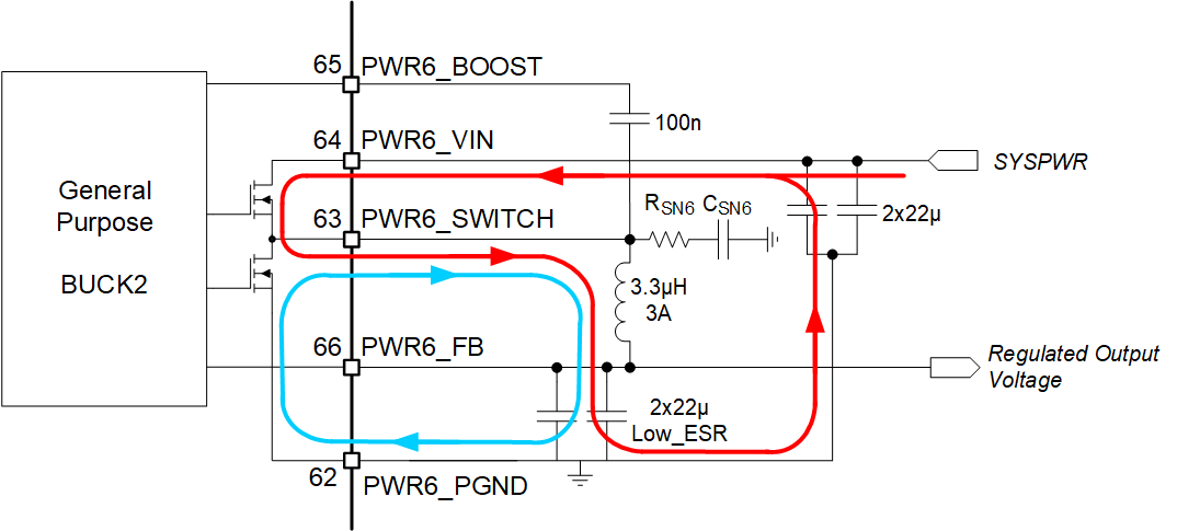
The high currents of the buck converters concentrate around pins VIN, SWITCH and PGND (Figure 11-1). The voltage at the pins VIN, PGND, and FB are DC voltages while the pin SWITCH has a switching voltage between VIN and PGND. In case the FET between pins 63 and 64 is closed, the red line indicates the current flow while the blue line indicates the current flow when the FET between pins 62 and 63 is closed. These paths carry the highest currents and must be kept as short as possible.
 Figure 11-1 High AC Current Paths in a
Buck Converter
Figure 11-1 High AC Current Paths in a
Buck ConverterThe trace to the VIN pin carries high AC currents. Therefore, the trace should be low-resistive to prevent voltage drop across the trace. Additionally, the decoupling capacitors should be placed as near to the VIN pin as possible.
The SWITCH pin is connected alternately to the VIN or GND. This means a square wave voltage is present on the SWITCH pin with an amplitude of VIN and containing high frequencies. This can lead to EMI problems if not properly handled. To reduce EMI problems a snubber network (RSN6 and CSN6) is placed at the SWITCH pin to prevent and/or suppress unwanted high-frequency ringing at the moment of switching.
The PGND pin sinks high current and should be connected to a star ground point such that it does not interfere with other ground connections.
The FB pin is the sense connection for the regulated output voltage, which is a DC voltage; no current is flowing through this pin. The voltage on the FB pin is compared with the internal reference voltage in order to control the loop. The FB connection should be made at the load such that I•R drop is not affecting the sensed voltage.