ZHCSE87A October 2015 – September 2023 DLPA3000
PRODUCTION DATA
- 1
- 1 特性
- 2 应用
- 3 说明
- 4 Revision History
- 5 说明(续)
- 6 Pin Configuration and Functions
- 7 Specifications
-
8 Detailed Description
- 8.1 Overview
- 8.2 功能方框图
- 8.3
Feature Description
- 8.3.1 Supply and Monitoring
- 8.3.2 Illumination
- 8.3.3 DMD Supplies
- 8.3.4 Buck Converters
- 8.3.5 Auxiliary LDOs
- 8.3.6 Measurement System
- 8.3.7 Digital Control
- 8.4 Device Functional Modes
- 8.5 Register Maps
- 9 Application and Implementation
- 10Power Supply Recommendations
- 11Layout
- 12Device and Documentation Support
- 13Mechanical, Packaging, and Orderable Information
封装选项
机械数据 (封装 | 引脚)
- PFD|100
散热焊盘机械数据 (封装 | 引脚)
- PFD|100
订购信息
11.6 Thermal Considerations
- Improving the heat sinking capability of the PCB
- Reducing thermal resistance to the environment of the chip by adding or increasing heat sink capability on top of the package
- Adding or increasing airflow in the system
The recommended junction temperature for the DLPA3000 is below 120°C during operation. The equation that relates junction temperature, Tjunction, is given by:

where Tambient is the ambient temperature, Pdiss is the total power dissipation, and RθJA is the thermal resistance from junction to ambient.
The total power dissipation may vary depending on the application of the DLPA3000. The main contributors in the DLPA3000 are typically:- Buck converters
- RGB strobe decoder switches
- LDOs
For the buck converter, the dissipated power is given by:
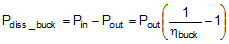
where ηbuck is the efficiency of the buck converter, Pin is the power delivered at the input of the buck converter, and Pout is the power delivered to the load of the buck converter. For the buck converter PWR1,2,6, the efficiency can be determined using the curves in Figure 7-22.
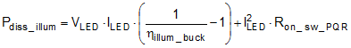
Similarly, for the buck converter in the illumination block, the dissipated power Pdiss_illum_buck can be calculated using the expression for Pdiss_buck. For the illumination block, an extra term needs to be added to the dissipation; that is, the dissipation of the LED switch. So, the dissipation for the illumination block, Pdiss_illum, can be described by:
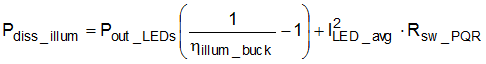
where Pout-LEDs represents the total power supplied to the LEDs, ILED_avg is the average LED current, and Rsw_PQR is the on-resistance of the RGB strobe controller switches. It should be noted here that the sense resistor, RLIM, also carries the average LED current, but it is not added to the equation of the dissipation for the illumination block. The RLIM is external to the DLPA3000 and it does not contribute the heat directly to the DLPA3000. For the total system dissipation, RLIM should be included.
For the LDO. the power dissipation is given by:

where Vin is the input supply voltage, Vout is the output voltage of the LDO, and Iload is the load current of the LDO.
The voltage drops over the LDO (Vin-Vout) can be relatively large; a small load current can result in significant power dissipation. For this situation, a general purpose buck converter can be a more efficient solution.The LDO DMD provides power to the boost converter, and the boost converter provides high voltages for the DMD; that is, VBIAS, VOFS, VRST. The current load on these lines can increase up to Iload,max=10 mA. Assuming the efficiency of the boost converter, ηboost, is 80%, the maximum boost converter power dissipation, Pdiss_DMD_boost,max, can be calculated as:

Compared to the power dissipation of the illumination buck converter, the power dissipation of the boost converter is negligible. However, the power dissipation of the LDO DMD, Pdiss_LDO_DMD should be given consideration in the case of a high supply voltage. The worst-case load current for the LDO is given by:
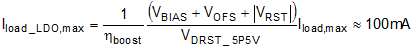
where the output voltage of the LDO is VDRST_5P5V= 5.5 V.
The worst-case power dissipation of the LDO DMD is approximately 1.5 W when the input supply voltage is 19.5 V. For your specific application, it is recommended to check the LDO current level. Therefore, the total power dissipation of the DLPA3000 can be described as:
The following examples calculate of the maximum ambient temperature and the junction temperature based on known information.
If it is assumed that the total dissipation Pdiss_DLPA3000 = 7.5 W, Tjunction,max= 120 °C, RθJA= 7 °C/W(refer to Thermal Information), then the maximum ambient temperature can be calculated using Equation 11:

If the total power dissipation and the ambient temperature are known as:
Tambient= 50 °C, RθJA= 7 °C/W, Pdiss_DLPA3000= 7.5 W.
the junction temperature can be calculated:

If the combination of ambient temperature and the total power dissipation of the DLPA3000 does not produce an acceptable junction temperature, that is, <120°C, there are two approaches:
- Using larger heat sink or more airflow to reduce RθJA
- Reduce power dissipation in
DLPA3000:
- Use an external buck converter instead of an internal general purpose buck converter.
- Reduce load current for the buck converter.
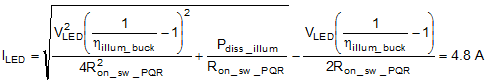
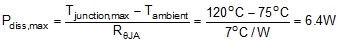
The following example shows how to calculate the maximum ILED at 6A when the junction temperature exceeds the maximum allowed temperature.. If it is assumed that Pbuck_converters= 1 W, PLDOs = 0.5 W, Tambient= 75°C, RθJA= 7°C/W, VLED= 3.5 V and Tjunction,max= 120°C, then the total maximum allowed dissipation for the DLPA3000 can be calculated:
The total dissipation for the buck converters and LDOs is 1.5W, so the maximum dissipation for the illumination block is 4.9W.
The efficiency of the converter can be determined from Figure 8-13. For VLED= 3.5 V and ILED is between 4 A and 6 A, the average efficiency is about 80%. The typically value of the on resistance of switch P,Q,R is 30 mOhm. Assuming VLED is independent of ILED, the ILED can be calculated using Equation 13: