ZHCSE87A October   2015  – September 2023 DLPA3000

PRODUCTION DATA  

  1.   1
  2. 特性
  3. 应用
  4. 说明
  5. Revision History
  6. 说明(续)
  7. Pin Configuration and Functions
  8. Specifications
    1. 7.1 Absolute Maximum Ratings
    2. 7.2 ESD Ratings
    3. 7.3 Recommended Operating Conditions
    4. 7.4 Thermal Information
    5. 7.5 Electrical Characteristics
    6. 7.6 SPI Timing Parameters
  9. Detailed Description
    1. 8.1 Overview
    2. 8.2 功能方框图
    3. 8.3 Feature Description
      1. 8.3.1 Supply and Monitoring
        1. 8.3.1.1 Supply
        2. 8.3.1.2 Monitoring
          1. 8.3.1.2.1 Block Faults
          2. 8.3.1.2.2 Low Battery and UVLO
          3. 8.3.1.2.3 Auto LED Turn Off Functionality
          4. 8.3.1.2.4 Thermal Protection
      2. 8.3.2 Illumination
        1. 8.3.2.1 Programmable Gain Block
        2. 8.3.2.2 LDO Illum
        3. 8.3.2.3 Illumination Driver A
        4. 8.3.2.4 RGB Strobe Decoder
          1. 8.3.2.4.1 Break Before Make (BBM)
          2. 8.3.2.4.2 Openloop Voltage
          3. 8.3.2.4.3 Transient Current Limit
        5. 8.3.2.5 Illumination Monitoring
          1. 8.3.2.5.1 Power Good
          2. 8.3.2.5.2 Ratio Metric Overvoltage Protection
        6. 8.3.2.6 Load Current and Supply Voltage
        7. 8.3.2.7 Illumination Driver Plus Power FETS Efficiency
      3. 8.3.3 DMD Supplies
        1. 8.3.3.1 LDO DMD
        2. 8.3.3.2 DMD HV Regulator
          1. 8.3.3.2.1 Power-Up and Power-Down Timing
        3. 8.3.3.3 DMD/DLPC Buck Converters
        4. 8.3.3.4 DMD Monitoring
          1. 8.3.3.4.1 Power Good
          2. 8.3.3.4.2 Overvoltage Fault
      4. 8.3.4 Buck Converters
        1. 8.3.4.1 LDO Bucks
        2. 8.3.4.2 General Purpose Buck Converters
        3. 8.3.4.3 Buck Converter Monitoring
          1. 8.3.4.3.1 Power Good
          2. 8.3.4.3.2 Overvoltage Fault
        4. 8.3.4.4 Buck Converter Efficiency
      5. 8.3.5 Auxiliary LDOs
      6. 8.3.6 Measurement System
      7. 8.3.7 Digital Control
        1. 8.3.7.1 SPI
        2. 8.3.7.2 Interrupt
        3. 8.3.7.3 Fast-Shutdown in Case of Fault
    4. 8.4 Device Functional Modes
    5. 8.5 Register Maps
  10. Application and Implementation
    1. 9.1 Application Information
    2. 9.2 Typical Applications
      1. 9.2.1 Typical Application Setup Using DLPA3000
        1. 9.2.1.1 Design Requirements
        2. 9.2.1.2 Detailed Design Procedure
        3. 9.2.1.3 Application Curve
      2. 9.2.2 Typical Application with DLPA3000 Internal Block Diagram
  11. 10Power Supply Recommendations
  12. 11Layout
    1. 11.1 Layout Guidelines
    2. 11.2 Layout Example
    3. 11.3 SPI Connections
    4. 11.4 RLIM Routing
    5. 11.5 LED Connection
    6. 11.6 Thermal Considerations
  13. 12Device and Documentation Support
    1. 12.1 第三方产品免责声明
    2. 12.2 Device Support
      1. 12.2.1 Device Nomenclature
    3. 12.3 Related Links
    4. 12.4 接收文档更新通知
    5. 12.5 支持资源
    6. 12.6 Trademarks
    7. 12.7 支持资源
    8. 12.8 静电放电警告
    9. 12.9 术语表
  14. 13Mechanical, Packaging, and Orderable Information

封装选项

机械数据 (封装 | 引脚)
散热焊盘机械数据 (封装 | 引脚)
订购信息

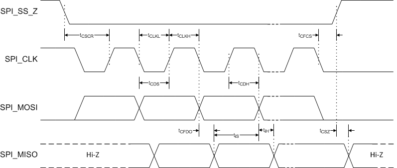
SPI Timing Parameters

SPI_VIN = 3.6 V, TA = 0 to 70°C, CL = 10 pF (unless otherwise noted).
PARAMETER MIN MAX UNIT
fCLK Serial clock frequency 0 40 MHz
tCLKL Pulse width low, SPI_CLK, 50% level 10 ns
tCLKH Pulse width high, SPI_CLK, 50% level 10 ns
tt Transition time, 20% to 80% level, all signals 0.2 4 ns
tCSCR SPI_SS_Z falling to SPI_CLK rising, 50% level 8 ns
tCFCS SPI_CLK falling to SPI_CSZ rising, 50% level 1 ns
tCDS SPI_MOSI data setup time, 50% level 7 ns
tCDH SPI_MOSI data hold time, 50% level 6 ns
tiS SPI_MISO data setup time, 50% level 10 ns
tiH SPI_MISO data hold time, 50% level 0 ns
tCFDO SPI_CLK falling to SPI_MISO data valid, 50% level 13 ns
tCSZ SPI_CSZ rising to SPI_MISO HiZ 6 ns
GUID-BFCE928D-8CAD-4819-AF5C-A7613E69320C-low.gif Figure 7-1 SPI Timing Diagram