ZHCSE87A October 2015 – September 2023 DLPA3000
PRODUCTION DATA
- 1
- 1 特性
- 2 应用
- 3 说明
- 4 Revision History
- 5 说明(续)
- 6 Pin Configuration and Functions
- 7 Specifications
-
8 Detailed Description
- 8.1 Overview
- 8.2 功能方框图
- 8.3
Feature Description
- 8.3.1 Supply and Monitoring
- 8.3.2 Illumination
- 8.3.3 DMD Supplies
- 8.3.4 Buck Converters
- 8.3.5 Auxiliary LDOs
- 8.3.6 Measurement System
- 8.3.7 Digital Control
- 8.4 Device Functional Modes
- 8.5 Register Maps
- 9 Application and Implementation
- 10Power Supply Recommendations
- 11Layout
- 12Device and Documentation Support
- 13Mechanical, Packaging, and Orderable Information
封装选项
机械数据 (封装 | 引脚)
- PFD|100
散热焊盘机械数据 (封装 | 引脚)
- PFD|100
订购信息
8.3.4.2 General Purpose Buck Converters
The buck converter is for general purpose use (Figure 8-20). The converter can be enabled or disabled through the Enable Register (0x01): BUCK_GP2_EN.
General purpose buck2 (PWR6) has a current capability of 2 A.
The buck converter can operate in two switching modes: normal (600-kHz switching frequency) mode and the skip mode. The skip mode is designed to increase light load efficiency. As the output current decreases from heavy load condition, the inductor current is also reduced and eventually comes to point that its rippled valley touches zero level, which is the boundary between continuous conduction and discontinuous conduction modes. The rectifying MOSFET is turned off when its zero inductor current is detected. As the load current further decreases, the converter runs into discontinuous conduction mode. The on-time is kept almost the same as it was in the continuous conduction mode so that it takes longer time to discharge the output capacitor with smaller load current to the level of the reference voltage.
The theory of operation of a buck converter is explained in Understanding Buck Power Stages in Switchmode Power Supplies. This section will therefore be limited to the component selection. For proper operation, selection of the external components is very important, especially the inductor LOUT and the output capacitor COUT. For best efficiency and ripple performance, an inductor and capacitor should be chosen with low equivalent series resistance (ESR).
The component selection of the buck converter is mainly determined by the output voltage. Table 8-3 shows the recommended value for inductor LOUT and capacitor COUT for a given output voltage.
| VOUT (V) | LOUT (µH) | COUT (µF) | |||
|---|---|---|---|---|---|
| MIN | TYP | MAX | MIN | MAX | |
| 1 – 1.5 | 1.0 | 2.2 | 4.7 | 10 | 132 |
| 1.5 – 3.3 | 2.2 | 3.3 | 4.7 | 22 | 68 |
| 3.3 – 5 | 3.3 | 4.7 | 22 | 68 | |
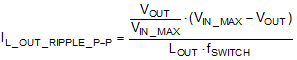
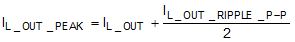
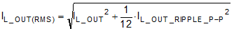
The inductor peak-to-peak ripple current, peak current, and RMS current can be calculated using Equation 6, Equation 7, and Equation 8, respectively. The inductor saturation current rating must be greater than the calculated peak current. Likewise, the RMS or heating current rating of the inductor must be greater than the calculated RMS current. The switching frequency of the buck converter is approximately 600 kHz (ƒSWITCH).
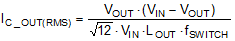
The capacitor value and ESR determines the level of output voltage ripple. The buck converter is intended for use with ceramic or other low ESR capacitors. Recommended values range from 22 μF to 68 μF. Equation 9 can be used to determine the required RMS current rating for the output capacitor.
Two other components need to be selected in the buck converter configuration. The value of the input-capacitor (pin PWRx_VIN) should be equal or greater than halve the selected output capacitance COUT. In this case CIN 2 × 10 µF is sufficient. The capacitor between PWRx_SWITCH and PWRx_BOOST is a charge pump capacitor to drive the high side FET. The recommended value is 100 nF.
Since the switching edges of the buck converter are relatively fast, voltage overshoot and ringing can become a problem. To overcome this problem a snubber network is used. The snubber circuit consists of a resistor and capacitor that are connected in series from the switch node to ground. The snubber circuit is used to damp the parasitic inductances and capacitances during the switching transitions. This circuit reduces the ringing voltage and also reduces the number of ringing cycles. The snubber network is formed by RSNx and CSNx. More information on controlling switch-node ringing in synchronous buck converters and configuring the snubber can be found in Analog Application Journal 2Q 2012.