ZHCSE87A October 2015 – September 2023 DLPA3000
PRODUCTION DATA
- 1
- 1 特性
- 2 应用
- 3 说明
- 4 Revision History
- 5 说明(续)
- 6 Pin Configuration and Functions
- 7 Specifications
-
8 Detailed Description
- 8.1 Overview
- 8.2 功能方框图
- 8.3
Feature Description
- 8.3.1 Supply and Monitoring
- 8.3.2 Illumination
- 8.3.3 DMD Supplies
- 8.3.4 Buck Converters
- 8.3.5 Auxiliary LDOs
- 8.3.6 Measurement System
- 8.3.7 Digital Control
- 8.4 Device Functional Modes
- 8.5 Register Maps
- 9 Application and Implementation
- 10Power Supply Recommendations
- 11Layout
- 12Device and Documentation Support
- 13Mechanical, Packaging, and Orderable Information
封装选项
机械数据 (封装 | 引脚)
- PFD|100
散热焊盘机械数据 (封装 | 引脚)
- PFD|100
订购信息
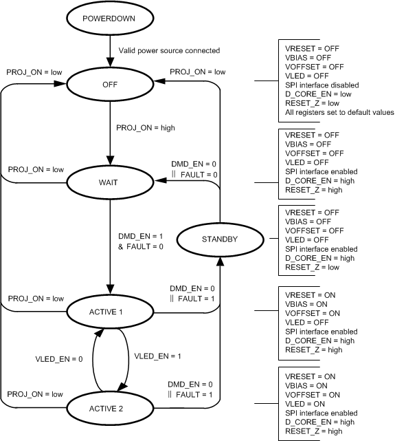
8.4 Device Functional Modes
Table 8-7 Modes of Operation
| MODE | DESCRIPTION |
|---|---|
| OFF | This is the lowest-power mode of operation. All power functions are turned off, registers are reset to their default values, and the IC does not respond to SPI commands. RESET_Z pin is pulled low. The IC will enter OFF mode whenever the PROJ_ON pin is low. |
| WAIT | The DMD regulators and LED power (VLED) are turned off, but the IC does respond to the SPI. The device enters WAIT mode whenever PROJ_ON is set high, DMD_EN(1) bit is set to 0 or a FAULT is resolved. |
| STANDBY | The device also enters STANDBY mode when a fault condition is detected. (2) (See Interrupt). Once the fault condition is resolved, WAIT mode is entered. |
| ACTIVE1 | The DMD supplies are enabled but LED power (VLED) is disabled. PROJ_ON pin must be high, DMD_EN bit must be set to 1, and ILLUM_EN(3) bit is set to 0. |
| ACTIVE2 | DMD supplies and LED power are enabled. PROJ_ON pin must be high and DMD_EN and ILLUM_EN bits must both be set to 1. |
(1) Settings can be done through Enable register, bit is named DMD_EN
(2) Power-good faults, overvoltage,
overtemperature
shutdown, and undervoltage lockout
(3) Settings can be done through register Enable register, bit is named ILLUM_EN
Table 8-8 Device State as a Function of
Control-Pin Status
| PROJ_ON Pin | STATE |
|---|---|
| LOW | OFF |
| HIGH | WAIT STANDBY ACTIVE1 ACTIVE2 (Device state depends on DMD_EN and ILLUM_EN bits and whether there are any fault conditions.) |

A. || = OR, & = AND
B. FAULT =
undervoltage
on any supply, thermal shutdown, or UVLO detection
C. UVLO detection, per the diagram,
causes the DLPA3000 to go into the standby state. This is not the lowest power
state. If lower power is desired, PROJ_ON should be set low.
D. DMD_EN register bit can be reset
or set by SPI writes. DMD_EN defaults to 0 when PROJ_ON goes from low to high
and then the DPP ASIC software automatically sets it to 1. Also, FAULT = 1
causes the DMD_EN register bit to be reset.
E. D_CORE_EN is a signal internal to
the DLPA3000. This signal turns on the VCORE regulator.
Figure 8-25 State
Diagram