ZHCSE87A October 2015 – September 2023 DLPA3000
PRODUCTION DATA
- 1
- 1 特性
- 2 应用
- 3 说明
- 4 Revision History
- 5 说明(续)
- 6 Pin Configuration and Functions
- 7 Specifications
-
8 Detailed Description
- 8.1 Overview
- 8.2 功能方框图
- 8.3
Feature Description
- 8.3.1 Supply and Monitoring
- 8.3.2 Illumination
- 8.3.3 DMD Supplies
- 8.3.4 Buck Converters
- 8.3.5 Auxiliary LDOs
- 8.3.6 Measurement System
- 8.3.7 Digital Control
- 8.4 Device Functional Modes
- 8.5 Register Maps
- 9 Application and Implementation
- 10Power Supply Recommendations
- 11Layout
- 12Device and Documentation Support
- 13Mechanical, Packaging, and Orderable Information
封装选项
机械数据 (封装 | 引脚)
- PFD|100
散热焊盘机械数据 (封装 | 引脚)
- PFD|100
订购信息
8.3.7.1 SPI
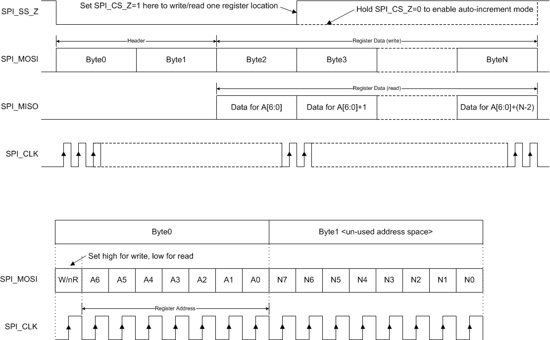
The DLPA3000 provides a 4-wire SPI port that supports two SPI clock frequency modes: 0 MHz to 36 MHz, and 20 MHz to 40 MHz. The interface supports both read and write operations. The SPI_SS_Z input serves as the active low chip select for the SPI port. The SPI_SS_Z input must be forced low for writing to or reading from registers. When SPI_SS_Z is forced high, the data at the SPI_MOSI input is ignored, and the SPI_MISO output is forced to a high-impedance state. The SPI_MOSI input serves as the serial data input for the port; the SPI_MISO output serves as the serial data output. The SPI_CLK input serves as the serial data clock for both the input and output data. Data at the SPI_MOSI input is latched on the rising edge of SPI_CLK, while data is clocked out of the SPI_MISO output on the falling edge of SPI_CLK. Figure 8-24 illustrates the SPI port protocol. Byte 0 is referred to as the command byte, where the most significant bit is the write/not-read bit. For the W/nR bit, a 1 indicates a write operation, while a 0 indicates a read operation. The remaining seven bits of the command byte are the register address targeted by the write or read operation. The SPI port supports write and read operations for multiple sequential register addresses through the implementation of an auto-increment mode. As shown in Figure 8-24, the auto-increment mode is invoked by simply holding the SPI_SS_Z input low for multiple data bytes. The register address is automatically incremented after each data byte transferred, starting with the address specified by the command byte. After reaching address 0x7Fh, the address pointer jumps back to 0x00h.
 Figure 8-24 SPI
Protocol