ZHCSGW5C January 2017 – March 2025 CC2640R2F-Q1
PRODUCTION DATA
- 1
- 1 特性
- 2 应用
- 3 说明
- 4 功能方框图
- 5 Device Comparison
- 6 Pin Configuration and Functions
-
7 Specifications
- 7.1 Absolute Maximum Ratings
- 7.2 ESD Ratings
- 7.3 Recommended Operating Conditions
- 7.4 Power Consumption Summary
- 7.5 General Characteristics
- 7.6 1Mbps GFSK (Bluetooth Low Energy Technology)—RX
- 7.7 1Mbps GFSK (Bluetooth Low Energy Technology)—TX
- 7.8 24MHz Crystal Oscillator (XOSC_HF)
- 7.9 32.768kHz Crystal Oscillator (XOSC_LF)
- 7.10 48MHz RC Oscillator (RCOSC_HF)
- 7.11 32kHz RC Oscillator (RCOSC_LF)
- 7.12 ADC Characteristics
- 7.13 Temperature Sensor
- 7.14 Battery Monitor
- 7.15 Continuous Time Comparator
- 7.16 Low-Power Clocked Comparator
- 7.17 Programmable Current Source
- 7.18 Synchronous Serial Interface (SSI)
- 7.19 DC Characteristics
- 7.20 Thermal Resistance Characteristics for RGZ Package
- 7.21 Timing Requirements
- 7.22 Switching Characteristics
- 7.23 Typical Characteristics
- 8 Detailed Description
- 9 Application, Implementation, and Layout
- 10Device and Documentation Support
- 11Revision History
- 12Mechanical, Packaging, and Orderable Information
9.1 Application Information
Very few external components are required for the operation of the CC2640R2F-Q1 device. This section provides general information about the differential configuration when using the CC2640R2F-Q1 device in an application, and an example application circuit with schematics and layout is shown in Figure 9-1, Figure 9-2, Figure 9-3, and Figure 9-4. This is only a small selection of the many application circuit examples available as complete reference designs from the product folder on www.ti.com.
Figure 9-1 shows the differential RF front-end configuration option with internal biasing. See the CC2640Q1EM-7ID reference design for this option.
 Figure 9-1 CC2640R2F-Q1 Application Circuit
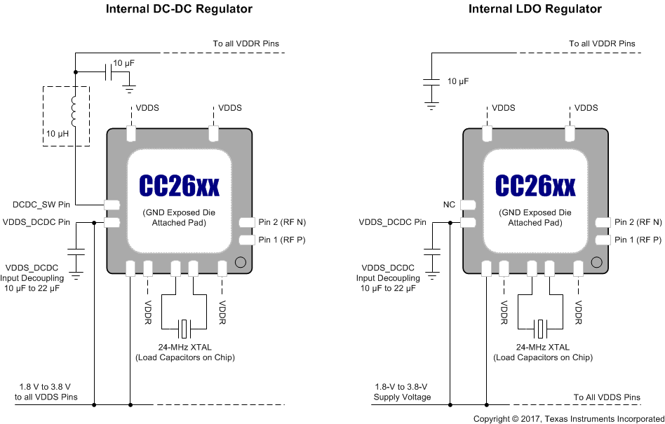
Figure 9-2 shows the various supply voltage configuration options for the CC2640R2F-Q1 device. Not all power supply decoupling capacitors or digital I/Os are shown. For a detailed overview of power supply decoupling and wiring, see the TI reference designs and the CC13x0, CC26x0 SimpleLink Wireless MCU Technical Reference Manual.
 Figure 9-2 Supply Voltage
Configurations