ZHCSNA1A april 2020 – february 2021 BQ25968
PRODUCTION DATA
- 1
- 1 特性
- 2 应用
- 3 说明
- 4 Revision History
- 5 说明(续)
- 6 Device Comparison Table
- 7 Pin Configuration and Functions
- 8 Specifications
-
9 Detailed Description
- 9.1 Overview
- 9.2 Functional Block Diagram
- 9.3
Feature Description
- 9.3.1 Charging System
- 9.3.2 Battery Charging Profile
- 9.3.3 Control State Diagram for System Implementation
- 9.3.4 Device Power Up
- 9.3.5 Switched Cap Function
- 9.3.6 Charging Start-Up
- 9.3.7 Integrated 16-Bit ADC for Monitoring and Smart Adapter Feedback
- 9.3.8 Device Internal Thermal Shutdown, TSBUS, and TSBAT Temperature Monitoring
- 9.3.9 INT Pin, STAT, FLAG, and MASK Registers
- 9.3.10 CDRVH and CDRVL_ADDRMS Functions
- 9.3.11 Parallel Operation Using Master and Slave Modes
- 9.4 Device Functional Modes
- 9.5 Programming
- 9.6 Register Maps
- 10Application and Implementation
- 11Power Supply Recommendations
- 12Layout
- 13Device and Documentation Support
- 14Mechanical, Packaging, and Orderable Information
9.3.8 Device Internal Thermal Shutdown, TSBUS, and TSBAT Temperature Monitoring
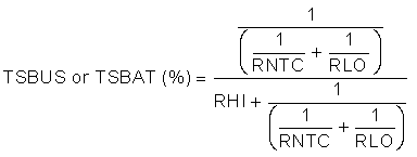
The device has three temperature sensing mechanisms to protect the device and system during charging: TSBUS for monitoring the cable connector temperature, TSBAT for monitoring the battery temperature, and TDIE for monitoring the internal junction temperature of the device. TSBUS and TSBAT only operate when there is a valid input supply. The TSBUS and TSBAT both rely on a resistor divider that has an external pullup voltage to VOUT. Place a negative coefficient thermistor in parallel to the low-side resistor. A fault on the TSBUS and TSBAT pin is triggered on the falling edge of the voltage threshold, signifying a “hot” temperature. The threshold is adjusted using the TSBUS_FLT and TSBAT_FLT registers. A warning TSBUS_TSBAT_ALM interrupt will be sent if the percentage reached within 5% of the FLT setting. If the TSBUS_FLT or TSBAT_FLT is disabled, it will not trigger a TSBUS_TSBAT_ALM interrupt. The RLO and RHI resistors should be chosen depending on the NTC used. If a 10-kΩ NTC is used, use 10-kΩ resistors for RLO and RHI. If a 100-kΩ NTC is used, use 100-kΩ resistors for RLO and RHI. The ratio of VTS/VOUT can be from 0% to 50%, and the voltage at the TS pin is determined by the following equation.
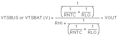
The percentage of the TS pin voltage is determined by the following equation.
Additionally, the device has an internal die temperature measurement, with adjustable threshold TDIE_FLT.
If TSBUS, TSBAT, or TDIE protections are not used, the functions can be disabled in the CHRG_CTRL register by setting the TSBUS_DIS, TSBAT_DIS, or TDIE_DIS bit to ‘1’. If the TSBUS_FLT, TSBAT_FLT, thresholds are reached, the CHG_EN bit is set to ‘0’, and the start-up sequence must be followed to resume charging.
Using the TDIE_ALM register, an alarm can be set to notify the host when the device die temperature exceeds a threshold. The device will not automatically stop switching when reaching the alarm threshold, and the host may decide on the steps to take to lower the temperature, such as reducing the charge current. The device will automatically stop switching when it reaches the TSHUT threshold.