ZHCSNA1A april 2020 – february 2021 BQ25968
PRODUCTION DATA
- 1
- 1 特性
- 2 应用
- 3 说明
- 4 Revision History
- 5 说明(续)
- 6 Device Comparison Table
- 7 Pin Configuration and Functions
- 8 Specifications
-
9 Detailed Description
- 9.1 Overview
- 9.2 Functional Block Diagram
- 9.3
Feature Description
- 9.3.1 Charging System
- 9.3.2 Battery Charging Profile
- 9.3.3 Control State Diagram for System Implementation
- 9.3.4 Device Power Up
- 9.3.5 Switched Cap Function
- 9.3.6 Charging Start-Up
- 9.3.7 Integrated 16-Bit ADC for Monitoring and Smart Adapter Feedback
- 9.3.8 Device Internal Thermal Shutdown, TSBUS, and TSBAT Temperature Monitoring
- 9.3.9 INT Pin, STAT, FLAG, and MASK Registers
- 9.3.10 CDRVH and CDRVL_ADDRMS Functions
- 9.3.11 Parallel Operation Using Master and Slave Modes
- 9.4 Device Functional Modes
- 9.5 Programming
- 9.6 Register Maps
- 10Application and Implementation
- 11Power Supply Recommendations
- 12Layout
- 13Device and Documentation Support
- 14Mechanical, Packaging, and Orderable Information
9.4.1.1 Input Overvoltage, Overcurrent, Undercurrent and Short-Circuit Protection
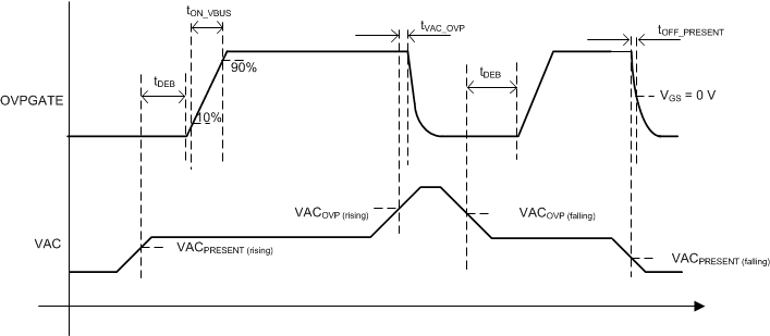
The device integrates the functionality of an input overvoltage protector. The device can be paired with an external N-channel FET to block input voltages higher than the setting programmed by the ADDR_MS pin. The device senses the input through the VAC pin and turns the external N-channel FET on or off through the OVPGATE pin. This eliminates the need for a separate OVP device to protect the overall system. The integrated VAC_OVP feature has a reaction time of tVAC_OVP. The VAC OVP setting is adjustable in the VAC_PROTECTION register.
The integrated OVP feature has a reaction time of tVAC_OVP (the actual time to turn off OVP FET will be longer and depends upon the FET gate capacitance) and the feature is always active as long as VVAC > VACPRESENT).
The default VAC OVP threshold is set by CDRVL_ADDRMS and can be changed with the VAC_PROTECTION register bits. VAC OVP bits are only reset by a REG_RST or a POR event where the CDRVL_ADDRMS value is used.
 Figure 9-8 OVPGATE Timing
The device has an integrated blocking FET (QB), with a reaction time of tVBUS_OVP. The BUS OVP threshold is adjustable in the BUS_OVP register.
Overcurrent protection monitors the current flow into VBUS. The overcurrent protection threshold is adjustable in the BUS_OCP register through the BUS_OCP bits, with a reaction time of tIBUS_OCP.
When any input OVP, UVP, or OCP event is triggered, the CHG_EN bit is set to ‘0’ to disable charging, and the start-up protocol must be followed to begin charging again.
When the BAT_UCP_ALM is triggered, the host is notified and the CHG_EN bit is not set to ‘0’ to disable charging. The host must disable charging after this event and determine when to switch back to the primary switching charger. This alarm is blanked during start up for proper operation. When the device starts switching, the IBUS_UCP protection is disabled until the BUS current rises above IBUS_UCP rising threshold. After that, if the BUS current falls below IBUS_UCP falling, the device will stop switching. IBUS_UCP falling threshold cannot be masked or disabled.