ZHCSNA1A april 2020 – february 2021 BQ25968
PRODUCTION DATA
- 1
- 1 特性
- 2 应用
- 3 说明
- 4 Revision History
- 5 说明(续)
- 6 Device Comparison Table
- 7 Pin Configuration and Functions
- 8 Specifications
-
9 Detailed Description
- 9.1 Overview
- 9.2 Functional Block Diagram
- 9.3
Feature Description
- 9.3.1 Charging System
- 9.3.2 Battery Charging Profile
- 9.3.3 Control State Diagram for System Implementation
- 9.3.4 Device Power Up
- 9.3.5 Switched Cap Function
- 9.3.6 Charging Start-Up
- 9.3.7 Integrated 16-Bit ADC for Monitoring and Smart Adapter Feedback
- 9.3.8 Device Internal Thermal Shutdown, TSBUS, and TSBAT Temperature Monitoring
- 9.3.9 INT Pin, STAT, FLAG, and MASK Registers
- 9.3.10 CDRVH and CDRVL_ADDRMS Functions
- 9.3.11 Parallel Operation Using Master and Slave Modes
- 9.4 Device Functional Modes
- 9.5 Programming
- 9.6 Register Maps
- 10Application and Implementation
- 11Power Supply Recommendations
- 12Layout
- 13Device and Documentation Support
- 14Mechanical, Packaging, and Orderable Information
9.3.5.1 Theory of Operation
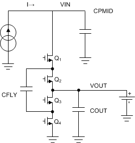
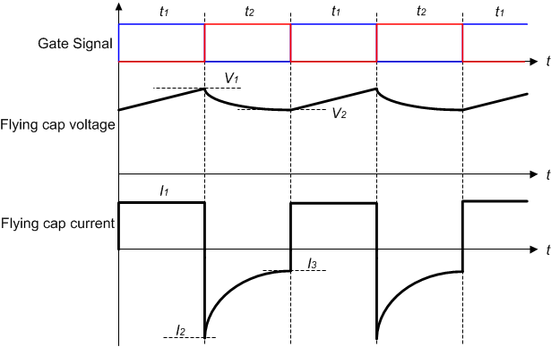
The power stage of the device is shown in the block diagram, and a simplified single phase circuit is shown in Figure 9-4. When operating, the device switches at a 50% duty cycle with Q1 and Q3 turned on and off at the same time, while Q2 and Q4 are turned on and off simultaneously. This results in the following equivalent circuits.
 Figure 9-4 BQ25968 Simplified Switched Cap Architecture (single phase)
 Figure 9-5 BQ25968 Equivalent Circuits During Operation
 Figure 9-6 BQ25968 Switching Waveforms