ZHCSNA1A april 2020 – february 2021 BQ25968
PRODUCTION DATA
- 1
- 1 特性
- 2 应用
- 3 说明
- 4 Revision History
- 5 说明(续)
- 6 Device Comparison Table
- 7 Pin Configuration and Functions
- 8 Specifications
-
9 Detailed Description
- 9.1 Overview
- 9.2 Functional Block Diagram
- 9.3
Feature Description
- 9.3.1 Charging System
- 9.3.2 Battery Charging Profile
- 9.3.3 Control State Diagram for System Implementation
- 9.3.4 Device Power Up
- 9.3.5 Switched Cap Function
- 9.3.6 Charging Start-Up
- 9.3.7 Integrated 16-Bit ADC for Monitoring and Smart Adapter Feedback
- 9.3.8 Device Internal Thermal Shutdown, TSBUS, and TSBAT Temperature Monitoring
- 9.3.9 INT Pin, STAT, FLAG, and MASK Registers
- 9.3.10 CDRVH and CDRVL_ADDRMS Functions
- 9.3.11 Parallel Operation Using Master and Slave Modes
- 9.4 Device Functional Modes
- 9.5 Programming
- 9.6 Register Maps
- 10Application and Implementation
- 11Power Supply Recommendations
- 12Layout
- 13Device and Documentation Support
- 14Mechanical, Packaging, and Orderable Information
9.3.11 Parallel Operation Using Master and Slave Modes
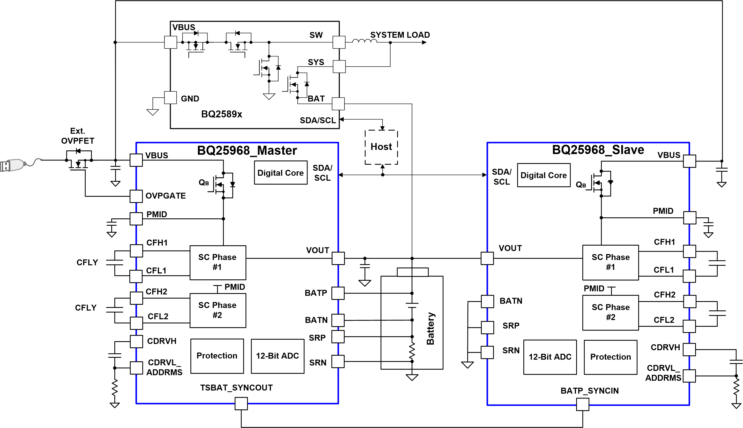
For higher power systems, it is possible to use two BQ25968 devices in parallel. This has the effect of reducing the adapter power requirements, reducing the cable losses, and reducing the losses in the device. The parallel system is shown in the figure below. The CDRVL_ADDRMS pin is used to configure the functionality of the device as Master or Slave. Refer to Section 9.3.10 for proper setting.
When configured as a Master, the TSBAT_SYNCOUT pin functions as SYNCOUT, and the BATP_SYNCIN pin functions as BATP. When configured as a Slave, the TSBAT_SYNCOUT pin functions as TSBAT, and the BATP_SYNCIN pin functions as SYNCIN. OVPGATE is controlled by the Master, and the OVPGATE pin on the slave should be left floating. Pull the SYNCIN/SYNCOUT pins to REGN through a 1-kΩ resistor.
 Figure 9-7 Parallel BQ25968 System