ZHCSW14C April 2008 – April 2024 AM26LV31E
PRODUCTION DATA
- 1
- 1 特性
- 2 应用
- 3 说明
- 4 Pin Configuration and Functions
- 5 Specifications
- 6 Parameter Measurement Information
- 7 Detailed Description
- 8 Application and Implementation
- 9 Device and Documentation Support
- 10Revision History
- 11Mechanical, Packaging, and Orderable Information
封装选项
机械数据 (封装 | 引脚)
散热焊盘机械数据 (封装 | 引脚)
订购信息
7.4 Device Functional Modes
Table 7-1 lists the functional modes of the AM26LV31E.
Table 7-1 Function Table
| INPUT A (1) | ENABLES | OUTPUTS | ||
|---|---|---|---|---|
| G | G | Y | Z | |
| H | H | X | H | L |
| L | H | X | L | H |
| H | X | L | H | L |
| L | X | L | L | H |
| X | L | H | Z | Z |
(1) H = high level, L = low level, X = irrelevant,
Z = high impedance (off)
Z = high impedance (off)
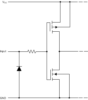
 Figure 7-2 Equivalent of Each Input (A, G, or
G) Schematic
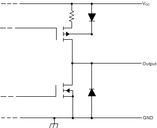
 Figure 7-3 Typical of Each Driver Output Schematic