ZHCSSI3 February 2024 ADS1288
PRODUCTION DATA
- 1
- 1 特性
- 2 应用
- 3 说明
- 4 Pin Configuration and Functions
-
5 Specifications
- 5.1 Absolute Maximum Ratings
- 5.2 ESD Ratings
- 5.3 Recommended Operating Conditions
- 5.4 Thermal Information
- 5.5 Electrical Characteristics
- 5.6 Timing Requirements: 1.65V ≤ IOVDD ≤ 1.95V and 2.7V ≤ IOVDD ≤ 3.6V
- 5.7 Switching Characteristics: 1.65V ≤ IOVDD ≤ 1.95V and 2.7V ≤ IOVDD ≤ 3.6V
- 5.8 Timing Diagrams
- 5.9 Typical Characteristics
- 6 Parameter Measurement Information
-
7 Detailed Description
- 7.1 Overview
- 7.2 Functional Block Diagram
- 7.3 Feature Description
- 7.4 Device Functional Modes
- 7.5
Programming
- 7.5.1 Serial Interface
- 7.5.2 Conversion Data Format
- 7.5.3
Commands
- 7.5.3.1 Single Byte Command
- 7.5.3.2 WAKEUP: Wake Command
- 7.5.3.3 STANDBY: Software Power-Down Command
- 7.5.3.4 SYNC: Synchronize Command
- 7.5.3.5 RESET: Reset Command
- 7.5.3.6 Read Data Direct
- 7.5.3.7 RDATA: Read Conversion Data Command
- 7.5.3.8 RREG: Read Register Command
- 7.5.3.9 WREG: Write Register Command
- 7.5.3.10 OFSCAL: Offset Calibration Command
- 7.5.3.11 GANCAL: Gain Calibration Command
-
8 Register Map
- 8.1
Register Descriptions
- 8.1.1 ID/SYNC: Device ID, SYNC Register (Address = 00h) [Reset = xxxx0010b]
- 8.1.2 CONFIG0: Configuration Register 0 (Address = 01h) [Reset = 92h]
- 8.1.3 CONFIG1: Configuration Register 1 (Address = 02h) [Reset = 10h]
- 8.1.4 HPF0, HPF1: High-Pass Filter Registers (Address = 03h, 04h) [Reset = 32h, 03h]
- 8.1.5 OFFSET0, OFFSET1, OFFSET2: Offset Calibration Registers (Address = 05h, 06h, 07h) [Reset = 00h, 00h, 00h]
- 8.1.6 GAIN0, GAIN1, GAIN2: Gain Calibration Registers (Address = 08h, 09h, 0Ah) [Reset = 00h, 00h, 40h]
- 8.1.7 GPIO: Digital Input/Output Register (Address = 0Bh) [Reset = 000xx000b]
- 8.1.8 SRC0, SRC1: Sample Rate Converter Registers (Address = 0Ch, 0Dh) [Reset = 00h, 80h]
- 8.1
Register Descriptions
- 9 Application and Implementation
- 10Device and Documentation Support
- 11Revision History
- 12Mechanical, Packaging, and Orderable Information
7.3.6.1 Sinc Filter Section
The first section of the digital filter is a variable-decimation, fifth-order sinc filter (sinx/x). Modulator data are passed through the sample rate converter to the sinc filter at the nominal rate of fMOD = fCLK / 4 = 1.024MHz. The sinc filter partially filters the data for the FIR filter that produces the final frequency response. The sinc filter output data are intended to be used with post-processing filters to shape the final frequency response.
Table 7-3 shows the decimation ratio and the resulting output data rate of the sinc filter. The sinc filter data rate is programmed by the DR[2:0] bits of the CONFIG0 register.
| DR[2:0] BITS | SINC DECIMATION RATIO (N) | DATA RATE (SPS) |
|---|---|---|
| 000 | 256 | 4,000 |
| 001 | 128 | 8,000 |
| 010 | 64 | 16,000 |
| 011 | 32 | 32,000 |
| 100 | 16 | 64,000 |
Equation 2 shows the Z-domain transfer function of the sinc filter.
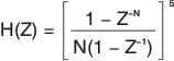
where:
- N = Decimation ratio of Table 7-3
Equation 3 shows the frequency domain transfer function of the sinc filter.
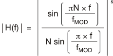
where:
- N = Decimation ratio shown in Table 7-3
- f = Input signal frequency
- fMOD = Modulator sampling frequency = fCLK / 4 (sample rate converter disabled)
The sinc filter frequency response has notches (or zeros) occurring at the output data rate and multiples thereof. At these frequencies, the filter has zero gain. Figure 7-11 shows the wide-band frequency response of the sinc filter and Figure 7-12 shows the –3dB response.
 Figure 7-11 Sinc Filter
Frequency Response
Figure 7-11 Sinc Filter
Frequency Response Figure 7-12 Sinc Filter
–3dB Response
Figure 7-12 Sinc Filter
–3dB ResponseFigure 7-13 shows the sinc filter frequency response at fDATA = 32kSPS. The tones at 1kHz and harmonics are the result of dither added to the modulator input to suppress idle tones. The frequency of the dither signal is fMOD divided by the combined decimation ratio from Table 7-4. The rise of the noise floor at 2kHz is resultant of modulator noise shaping. For sinc filter decimation N = 32 (data rate = 32kSPS), the usable bandwidth through the use of external post filtering is 500Hz.
") Figure 7-13 FFT Output of the Sinc Filter
(fDATA = 32kSPS)
Figure 7-13 FFT Output of the Sinc Filter
(fDATA = 32kSPS)The sinc filter data bypasses the data scaling, clip stage, and user calibration stages, and as a result, the sinc filter data are scaled differently compared to the FIR filter data. See the Conversion Data Format section for details of sinc filter data scaling.