ZHCSN14H June   2005  – June 2025 ADS1232 , ADS1234

PRODUCTION DATA  

  1.   1
  2. 特性
  3. 应用
  4. 说明
  5. Pin Configuration and Functions
  6. Specifications
    1. 5.1 Absolute Maximum Ratings
    2. 5.2 ESD Ratings
    3. 5.3 Recommended Operating Conditions
    4. 5.4 Thermal Information
    5. 5.5 Electrical Characteristics
    6. 5.6 Typical Characteristics
  7. Parameter Measurement Information
    1. 6.1 Noise Performance
  8. Detailed Description
    1. 7.1 Overview
    2. 7.2 Functional Block Diagram
    3. 7.3 Feature Description
      1. 7.3.1  Analog Inputs (AINPX, AINNX)
      2. 7.3.2  Temperature Sensor (ADS1232 Only)
      3. 7.3.3  Low-Noise PGA
        1. 7.3.3.1 PGA Bypass Capacitor
      4. 7.3.4  Voltage Reference Inputs (REFP, REFN)
      5. 7.3.5  Clock Sources
      6. 7.3.6  Digital Filter Frequency Response
      7. 7.3.7  Settling Time
      8. 7.3.8  Data Rate
      9. 7.3.9  Data Format
      10. 7.3.10 Data Ready and Data Output (DRDY/DOUT)
      11. 7.3.11 Serial Clock Input (SCLK)
      12. 7.3.12 Data Retrieval
    4. 7.4 Device Functional Modes
      1. 7.4.1 Offset Calibration Mode
      2. 7.4.2 Standby Mode
      3. 7.4.3 Standby Mode With Offset-Calibration
      4. 7.4.4 Power-Down Mode
      5. 7.4.5 Power-Up Sequence
      6. 7.4.6 Summary of Serial Interface Waveforms
  9. Application and Implementation
    1. 8.1 Application Information
    2. 8.2 Typical Application
      1. 8.2.1 Design Requirements
      2. 8.2.2 Detailed Design Procedure
      3. 8.2.3 Application Curves
    3. 8.3 Power Supply Recommendations
      1. 8.3.1 Power-Supply Decoupling
    4. 8.4 Layout
      1. 8.4.1 Layout Guidelines
      2. 8.4.2 Layout Example
  10. Device and Documentation Support
    1. 9.1 接收文档更新通知
    2. 9.2 支持资源
    3. 9.3 Trademarks
    4. 9.4 静电放电警告
    5. 9.5 术语表
  11. 10Revision History
  12. 11Mechanical, Packaging, and Orderable Information

封装选项

机械数据 (封装 | 引脚)
散热焊盘机械数据 (封装 | 引脚)
订购信息

Typical Characteristics

at TA = 25°C, AVDD = DVDD = V(REFP) = 5V, and V(REFN) = AGND (unless otherwise noted)

ADS1232 ADS1234 Noise Plot
 
Figure 5-1 Noise Plot
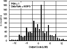
ADS1232 ADS1234 Noise Histogram
 
Figure 5-3 Noise Histogram
ADS1232 ADS1234 Noise Plot
 
Figure 5-5 Noise Plot
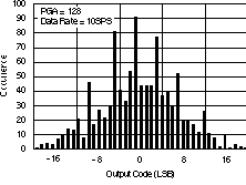
ADS1232 ADS1234 Noise Histogram
 
Figure 5-7 Noise Histogram
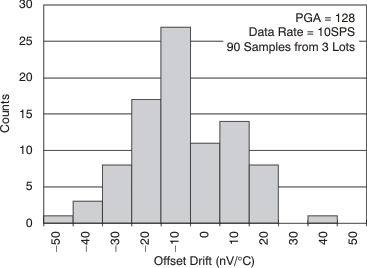
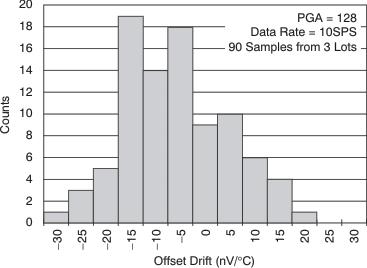
ADS1232 ADS1234 Offset Drift (–40°C to +25°C)
 
Figure 5-9 Offset Drift (–40°C to +25°C)
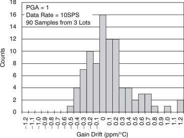
ADS1232 ADS1234 Gain Drift (–40°C to +25°C)
 
Figure 5-11 Gain Drift (–40°C to +25°C)
ADS1232 ADS1234 Offset Drift (–40°C to +25°C)
 
Figure 5-13 Offset Drift (–40°C to +25°C)
ADS1232 ADS1234 Gain Drift (–40°C to +25°C)
 
Figure 5-15 Gain Drift (–40°C to +25°C)
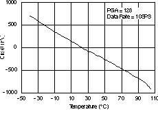
ADS1232 ADS1234 Offset vs Temperature
 
Figure 5-17 Offset vs Temperature
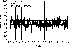
ADS1232 ADS1234 Noise vs Input Signal
 
Figure 5-19 Noise vs Input Signal
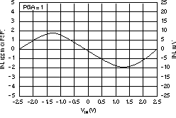
ADS1232 ADS1234 Integral Nonlinearity vs Input Signal
 
Figure 5-21 Integral Nonlinearity vs Input Signal
ADS1232 ADS1234 Analog Supply Current vs
                        Temperature
 
Figure 5-23 Analog Supply Current vs Temperature
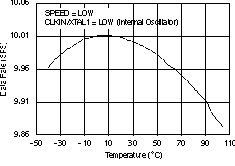
ADS1232 ADS1234 Data Rate vs Temperature
 
Figure 5-25 Data Rate vs Temperature
ADS1232 ADS1234 Noise Plot
 
Figure 5-2 Noise Plot
ADS1232 ADS1234 Noise Histogram
 
Figure 5-4 Noise Histogram
ADS1232 ADS1234 Noise Plot
 
Figure 5-6 Noise Plot
ADS1232 ADS1234 Noise Histogram
 
Figure 5-8 Noise Histogram
ADS1232 ADS1234 Offset Drift (25°C to 105°C)
 
Figure 5-10 Offset Drift (25°C to 105°C)
ADS1232 ADS1234 Gain Drift (25°C to 105°C)
 
Figure 5-12 Gain Drift (25°C to 105°C)
ADS1232 ADS1234 Offset Drift (25°C to 105°C)
 
Figure 5-14 Offset Drift (25°C to 105°C)
ADS1232 ADS1234 Gain Drift (25°C to 105°C)
 
Figure 5-16 Gain Drift (25°C to 105°C)
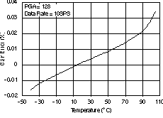
ADS1232 ADS1234 Gain Error vs Temperature
 
Figure 5-18 Gain Error vs Temperature
ADS1232 ADS1234 Noise vs Input Signal
 
Figure 5-20 Noise vs Input Signal
ADS1232 ADS1234 Integral Nonlinearity vs Input Signal
 
Figure 5-22 Integral Nonlinearity vs Input Signal
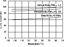
ADS1232 ADS1234 Digital Supply Current vs
                        Temperature
 
Figure 5-24 Digital Supply Current vs Temperature