TIDUCL3 February 2017
- 1 Overview
- 2 Resources
- 3 Features
- 4 Applications
- 5 Design Images
- 6 System Overview
-
7 System Design Theory
- 7.1 PCB and Form Factor
- 7.2 Optimizing Board Performance Based on LED String Voltage and Current
- 7.3 Switching Frequency
- 7.4 Output Overvoltage Protection (OVP)
- 7.5 Current Monitoring (IMON)
- 7.6 Thermal Foldback
- 7.7 Clock Generation (PWM)
- 7.8 Onboard Supply and Setting Duty Cycle
- 7.9 Buffering, Averaging, and Filtering
- 7.10 Boost Converter
- 8 Getting Started Hardware
- 9 Testing and Results
- 10Design Files
- 11Related Documentation
- 12About the Author
6.4.2 TLC555-Q1
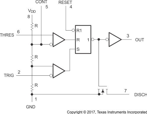
The TLC555 is a monolithic-timing circuit fabricated using the TI LinCMOS process (see Figure 3). The timer is fully compatible with CMOS, TTL, and MOS logic and operates at frequencies up to 2 MHz. Because of the high input impedance of this device, it uses smaller timing capacitors than those used by the NE555 device. As a result, more accurate time delays and oscillations are possible. Power consumption is low across the full range of power-supply voltage. The advantage of the TLC555-Q1 is that it exhibits greatly reduced supply-current spikes during output transitions. Although the CMOS output is capable of sinking over 100 mA and sourcing over 10 mA, the main reason the TLC555-Q1 is able to have low current spikes is because of its edge rates. This feature minimizes the requirement for the large decoupling capacitors required by the NE555.
 Figure 3. TLC555-Q1 Functional Block Diagram