TIDUCL3 February 2017
- 1 Overview
- 2 Resources
- 3 Features
- 4 Applications
- 5 Design Images
- 6 System Overview
-
7 System Design Theory
- 7.1 PCB and Form Factor
- 7.2 Optimizing Board Performance Based on LED String Voltage and Current
- 7.3 Switching Frequency
- 7.4 Output Overvoltage Protection (OVP)
- 7.5 Current Monitoring (IMON)
- 7.6 Thermal Foldback
- 7.7 Clock Generation (PWM)
- 7.8 Onboard Supply and Setting Duty Cycle
- 7.9 Buffering, Averaging, and Filtering
- 7.10 Boost Converter
- 8 Getting Started Hardware
- 9 Testing and Results
- 10Design Files
- 11Related Documentation
- 12About the Author
7.6.1.1 Changing Starting Point for Thermal Foldback
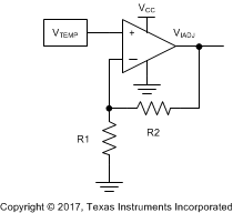
The TPS92691-Q1 has an internal clamp on the "IADJ" pin at 2.55 V and an absolute maximum input voltage at the pin of 8.8 V. Because there is room there to scale up the input into the "IADJ" pin, the simplest way to change the starting point for thermal foldback is introducing a non-inverting amplifier, as shown in Figure 11, with a gain found using Equation 9.
 Figure 11. Non-Inverting Amplifier
With an output voltage from the LMT87 of 3.16 V at –40°C, the maximum scaling factor possible is 2.5 in order to not violate the maximum voltage at the "IADJ" pin. Therefore, if a scaling factor of 2.5 was used, the temperature at which the current would start to derate would be 117ºC. Also if no scaling is used, the temperature at which the current starts to derate is 7ºC. Equation 10 and Equation 11 show how to choose at what temperature the derating should start.
NOTE
This is a first-order linear approximation. If being exact is required, consult the LMT87-Q1 datasheet.
Temperature range from –40°C to T:

Temperature range from T to 125°C:

Where "T" is the temperature when the current will start derating and K is the scaling factor introduced by the non-inverting amplifier. The scaling factor needed is determined by Equation 12:

Using these equations, the derating is set so that it occurs at whatever temperature chosen ±3°C. In order to build this application, choose an op amp specifically for this non-inverting amplifier. There are several factors that will effect which op amp would be a good candidate. The input offset specification is the key factor on how accurately the current would reflect the temperature. This would mean an op amp like the OP07 or LT1013. Another aspect would be a low common-mode input voltage with rail-to-rail output so that the VTEMP could go down to GND and the output of the op amp would accurately reflect that. Op amps such as the TLV341 or the OP314 would work in this case.