TIDUCL3 February 2017
- 1 Overview
- 2 Resources
- 3 Features
- 4 Applications
- 5 Design Images
- 6 System Overview
-
7 System Design Theory
- 7.1 PCB and Form Factor
- 7.2 Optimizing Board Performance Based on LED String Voltage and Current
- 7.3 Switching Frequency
- 7.4 Output Overvoltage Protection (OVP)
- 7.5 Current Monitoring (IMON)
- 7.6 Thermal Foldback
- 7.7 Clock Generation (PWM)
- 7.8 Onboard Supply and Setting Duty Cycle
- 7.9 Buffering, Averaging, and Filtering
- 7.10 Boost Converter
- 8 Getting Started Hardware
- 9 Testing and Results
- 10Design Files
- 11Related Documentation
- 12About the Author
7.10 Boost Converter
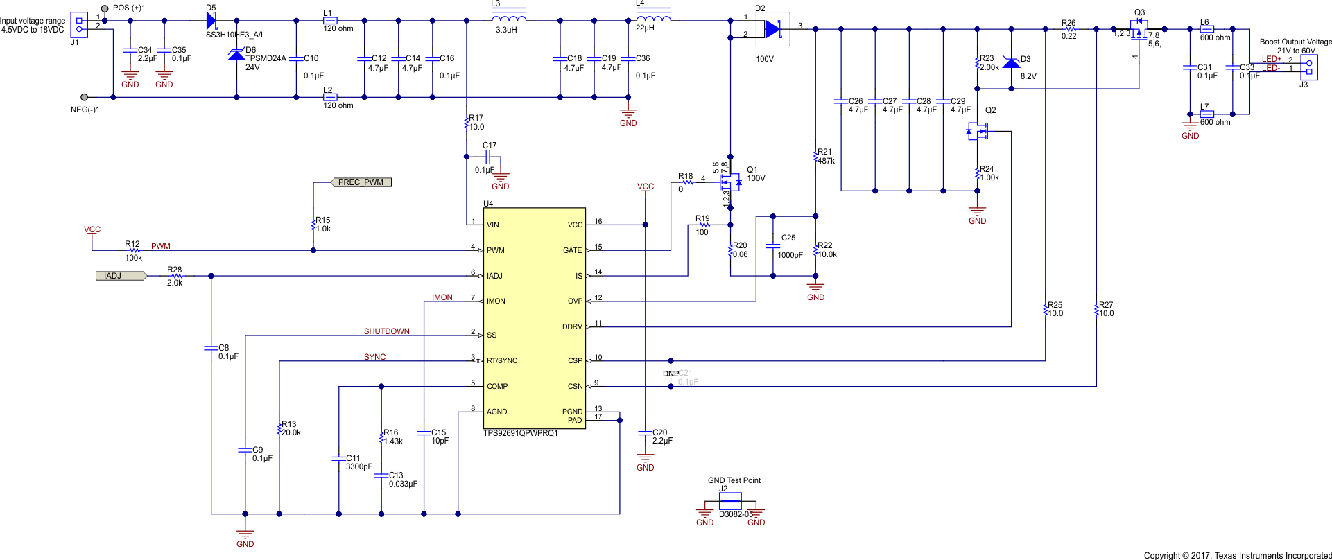
The TPS92691-Q1 controller is suitable for implementing step-up or step-down LED driver topologies (see Figure 22). This TI Design uses the boost configuration. Use the detailed design procedure of the device datasheet[2] to select component values for the TPS92691-Q1 device. This section addresses the design process for the boost converter.
 Figure 22. TPS92691-Q1 LED Driver in Boost Configuration
 DC-DC converters can couple large amounts of energy (especially at the fundamental switching frequency) back through the battery inputs and into the remainder of the vehicle. This energy is produced because of the switching action of the input-current waveform that is translated into voltage noise by the equivalent series resistance (ESR) of the input capacitors that carry most of this current. A low-pass filter, placed between the input of the module and the DC-DC converters, has been added to attenuate this noise. The low-pass filter also filters incoming noise that enters the system. The low-pass filter can be designed empirically or theoretically (by calculation and simulation). The empirical approach is to design the system without the EMI filter, measure the conducted emissions with a spectrum analyzer, and compare it to the standard that must be passed. Next, calculate the attenuation required to pass at certain frequencies and place the corner frequency of the filter low enough to achieve the desired attenuation.
The theoretical approach is more complicated. Ensure the assumption is that the boost converter is the problem and that the noise generated by the downstream circuitry is to be filtered by the boost inductor or capacitors.
NOTE
The main sources of noise are fundamental at the switching frequency of the boost
(400 kHz) and the harmonics. If the amplitude of the noise at that frequency can be estimated and attenuated appropriately, the harmonics can also be attenuated.
The input voltage is the voltage generated by the ripple current through the ESR of the input capacitors. Because ceramic capacitors are used, this ESR is very low (approximately 3 mΩ). The peak amplitude of the input voltage ripple is approximately 2.7 mV (see Equation 19). The concern is the frequency content at 400 kHz, not the time domain.

Use the Fourier transform of this asymmetric-triangle waveform to find the coefficients and amplitudes of each component frequency. The coefficient of the fundamental for this type of waveform is 0.8. Multiply the coefficient times the time domain amplitude to find the energy at 400 kHz (see Equation 20).

Using Equation 21, convert the product of Equation 20 to dBμV to make it easier to analyze based on the CISPR 25 standards.

Compare the 67 dBμV to the CISPR 25 specification and calculate how much to attenuate. The CISPR 25 specification does not define a limit at 400 kHz, but the limit at 530 kHz for Class 5 conducted emissions is 54 dBμV (peak). An attenuation of at least 13 dB is required. Make the goal 40-dB attenuation at the switching frequency. Calculate where to place the corner frequency of the filter when attenuation at 400 kHz is known. The second-order low-pass filter has a rolloff of –40 dB per decade. Place the corner frequency at 40 kHz to attain 40 dB of attenuation at 400 kHz. The corner frequency is related to the values of the filter inductor and capacitor, calculated by using Equation 22:

Choose an L of 3.3 µH. There is approximately 47 nF, calculating out for C. To keep the ESR low, put two capacitors in parallel and choose 4.7 μF for C12, C14 and C18, C19. Choosing a larger value lowers the corner frequency of the filter, which provides more attenuation at 400 kHz. Also, ceramic capacitors suffer from DC bias effects and operate at a capacitance that is less than their rating. To filter the high-frequency noise content, a 100-nF capacitor is added.