TIDUCL3 February 2017
- 1 Overview
- 2 Resources
- 3 Features
- 4 Applications
- 5 Design Images
- 6 System Overview
-
7 System Design Theory
- 7.1 PCB and Form Factor
- 7.2 Optimizing Board Performance Based on LED String Voltage and Current
- 7.3 Switching Frequency
- 7.4 Output Overvoltage Protection (OVP)
- 7.5 Current Monitoring (IMON)
- 7.6 Thermal Foldback
- 7.7 Clock Generation (PWM)
- 7.8 Onboard Supply and Setting Duty Cycle
- 7.9 Buffering, Averaging, and Filtering
- 7.10 Boost Converter
- 8 Getting Started Hardware
- 9 Testing and Results
- 10Design Files
- 11Related Documentation
- 12About the Author
7.9 Buffering, Averaging, and Filtering
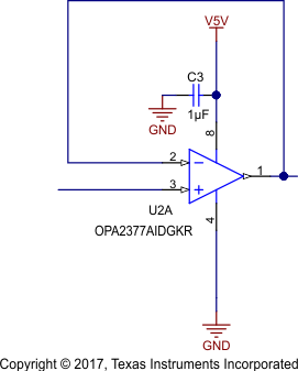
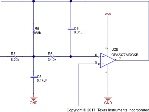
The OPA2377-Q1 dual op amp, low-noise, rail-to-rail input and output, and low offset, makes this device ideal for these type of applications. The output stage of the TLE555-Q1 as Section 6.4.2 describes is hooked up through a 1-K resistor to the PWM input of the TPS92691 device, which dims the LEDs and also connects to a buffer stage and a second-order filter formed by the dual OPA2377 op amp (see Figure 20). The buffer stage is placed to avoid changing impedance from input to output so as not to interfere with the shape or timing of the square wave generated by the TLC555. The waveform after the buffer stage is then averaged by the next op amp stage, which forms a second-order filter that is compared against a reverence voltage set by the resistor divider from the precision reference. The output of the second-order filter is hooked up to the CONT pin of the TLC555-Q1 closing the loop. The CONT input of the TLC555 allows the upper and lower trigger threshold of the timing duty cycle to be changed by varying the voltage level at this pin, which is performed by the output of the second-order filter.
 Figure 20. Buffer
 Use the following parameters for this TI Design example:
- Gain = 19.2 V/V (inverting gain)
- Low-pass cutoff frequency = 31.67 Hz
- Second-order Chebyshev filter response with a 3-dB gain peaking in the passband
Figure 21 shows the infinite-gain multiple-feedback circuit for a low-pass network function.
 Figure 21. Second-Order Filter and Averaging
 Use Equation 17 to calculate the voltage transfer function:

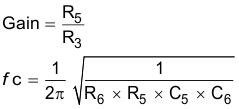
This circuit produces a signal inversion. For this circuit, the gain at DC and the low-pass cutoff frequency are calculated by Equation 18:

Where:
- Gain = 19.2
- fc = 31.67 Hz
Software tools are readily available to simplify filter design. WEBENCH® Filter Designer is a simple, powerful, and easy-to-use active filter design program. This program enables designers to create optimized filter designs using a selection of TI op amps and passive components from TI's vendor partners.