TIDUCL3 February 2017
- 1 Overview
- 2 Resources
- 3 Features
- 4 Applications
- 5 Design Images
- 6 System Overview
-
7 System Design Theory
- 7.1 PCB and Form Factor
- 7.2 Optimizing Board Performance Based on LED String Voltage and Current
- 7.3 Switching Frequency
- 7.4 Output Overvoltage Protection (OVP)
- 7.5 Current Monitoring (IMON)
- 7.6 Thermal Foldback
- 7.7 Clock Generation (PWM)
- 7.8 Onboard Supply and Setting Duty Cycle
- 7.9 Buffering, Averaging, and Filtering
- 7.10 Boost Converter
- 8 Getting Started Hardware
- 9 Testing and Results
- 10Design Files
- 11Related Documentation
- 12About the Author
7.7 Clock Generation (PWM)
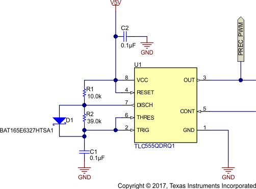
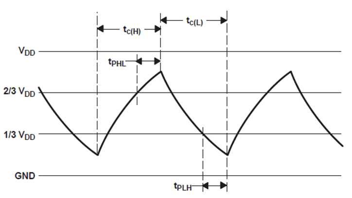
Connecting TRIG to THRES, as Figure 17 shows, causes the timer to run as a multivibrator. The capacitor C1 charges through R1 and D1 to the threshold voltage level (approximately 0.67 VDD) and then discharges through R2 only to the value of the trigger voltage level (approximately 0.33 VDD). As Figure 18 shows, the output is high during the charging cycle (tc(H)) and low during the discharge cycle (tc(L)).
 Figure 17. TLC555-Q1 Clock Generation
  Figure 18. Trigger and Threshold Voltage Waveform
 The values of R1, D1, R2, and C1 control the duty cycle, as the following equations show:


- tc(H) = 100 nF × 10 kΩ × ln 2 = 693 µs
- tc(L) = 100 nF × 39 kΩ × ln 2 = 2.7 ms
- Period = tc(H) + tc(L) = 3.39 ms
- Output waveform duty cycle = 20.4%
The preceding formulas do not allow for any propagation delay times from the TRIG and THRES inputs to DISCH. These delay times add directly to the period and create differences between calculated and actual values that increase with frequency. In addition, the internal ON-state resistance (rON) during discharge adds to R2 to provide another source of timing error in the calculation when R2 is very low or rON is very high. These errors can be canceled out by applying a feedback loop.