ZHCSMQ0I october 2004 – may 2023 TPS715-Q1
PRODUCTION DATA
- 1
- 1 特性
- 2 应用
- 3 说明
- 4 Revision History
- 5 Pin Configuration and Functions
- 6 Specifications
- 7 Detailed Description
- 8 Application and Implementation
- 9 Device and Documentation Support
- 10Mechanical, Packaging, and Orderable Information
8.2.2 Application Curves
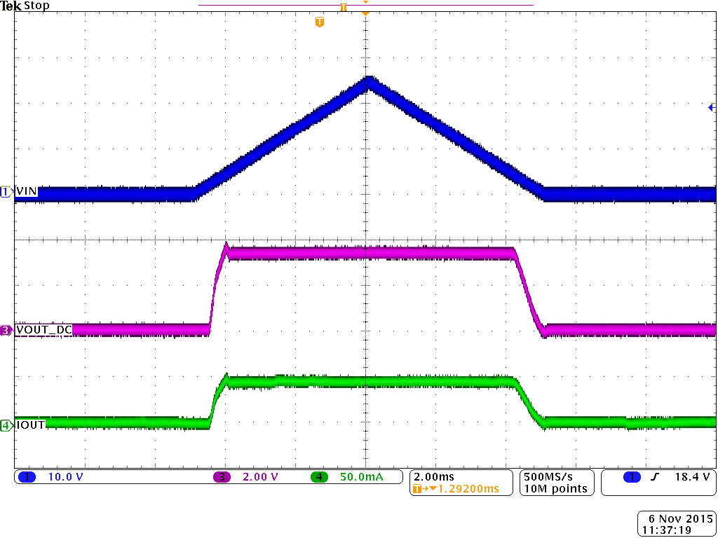
Figure 8-5 illustrates the input voltage ramp from 0 V to just below 24 V (CH1), the 3.3-V regulated output voltage (CH3), and the 50-mA output current (CH4). The scale on CH4 is 50 mA/div.
Figure 8-6 illustrates the input voltage ramp from 0 V to 8 V, the 3.3-V regulated output voltage, and the 50-mA output current.
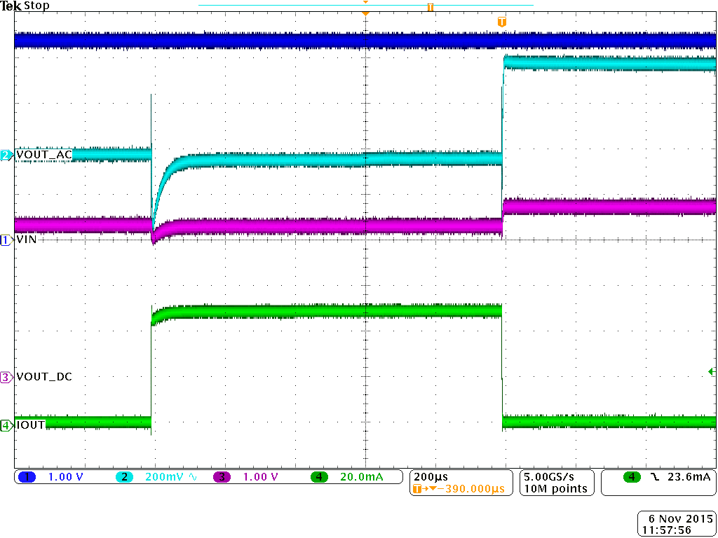
Figure 8-7 illustrates the load transient waveform of the TPS71533-Q1, output current is switched between 0 mA and 50 mA (CH4). Input voltage is set at 4.3 V (CH1). Output voltage DC (CH3) and output voltage AC (CH2) are also illustrated in the waveform.
Figure 8-8 illustrates the load transient waveform of the TPS71533-Q1, output current is switched between 0 mA and 50 mA with a slew rate of 0.5 A/μs. Input voltage is set at 4.3 V. Output voltage AC is illustrated in the waveform to capture the undershoot and overshoot behavior.
Figure 8-9 illustrates the line transient waveform of the TPS71533-Q1, where input voltage is switched between 5 V and 14 V with slew rate of 0.66 V/μs. Load current is set at 50 mA. Output voltage AC is illustrated in the waveform to capture the undershoot and overshoot behavior.
Figure 8-10 illustrates the fast dropout exit waveform of the TPS71533-Q1, where input voltage is switched between 2.5 V and 14 V with slew rate of 1.15 V/μs. Load current is set at 1 mA and 50 mA. Output voltage AC is illustrated in the waveform to capture the undershoot and overshoot behavior.
 Figure 8-5 TPS71533-Q1 Power-Up and Power-Down Waveform for Legacy Chip
 Figure 8-7 TPS71533-Q1 Load Transient Waveform for Legacy Chip
 Figure 8-9 TPS71533-Q1 Fast Line Transient Waveform for New Chip
 Figure 8-6 TPS71533-Q1 Power-Up and Power-Down Waveform for New Chip
 Figure 8-8 TPS71533-Q1 Load Transient Waveform for New Chip
 Figure 8-10 TPS71533-Q1 Dropout Exit Transient Response for New Chip