ZHCSF94E February 2018 – July 2020 LMR23625
PRODUCTION DATA
- 1 特性
- 2 应用
- 3 说明
- 4 Revision History
- 5 Pin Configuration and Functions
- 6 Specifications
-
7 Detailed Description
- 7.1 Overview
- 7.2 Functional Block Diagram
- 7.3
Feature Description
- 7.3.1 Fixed-Frequency Peak-Current-Mode Control
- 7.3.2 Adjustable Output Voltage
- 7.3.3 Enable/Sync
- 7.3.4 VCC, UVLO
- 7.3.5 Minimum ON-time, Minimum OFF-time and Frequency Foldback at Drop-out Conditions
- 7.3.6 Internal Compensation and CFF
- 7.3.7 Bootstrap Voltage (BOOT)
- 7.3.8 Overcurrent and Short-Circuit Protection
- 7.3.9 Thermal Shutdown
- 7.4 Device Functional Modes
-
8 Application and Implementation
- 8.1 Application Information
- 8.2
Typical Applications
- 8.2.1 Design Requirements
- 8.2.2
Detailed Design Procedure
- 8.2.2.1 Custom Design With WEBENCH® Tools
- 8.2.2.2 Output Voltage Setpoint
- 8.2.2.3 Switching Frequency
- 8.2.2.4 Inductor Selection
- 8.2.2.5 Output Capacitor Selection
- 8.2.2.6 Feed-forward Capacitor
- 8.2.2.7 Input Capacitor Selection
- 8.2.2.8 Bootstrap Capacitor Selection
- 8.2.2.9 VCC Capacitor Selection
- 8.2.2.10 Undervoltage Lockout Set-Point
- 8.2.3 Application Curves
- 9 Power Supply Recommendations
- 10Layout
- 11Device and Documentation Support
- 12Mechanical, Packaging, and Orderable Information
封装选项
请参考 PDF 数据表获取器件具体的封装图。
机械数据 (封装 | 引脚)
- DRR|12
- DDA|8
散热焊盘机械数据 (封装 | 引脚)
订购信息
8.2.2.10 Undervoltage Lockout Set-Point
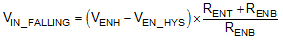
The system undervoltage lockout (UVLO) is adjusted using the external voltage divider network of RENT and RENB. The UVLO has two thresholds, one for power up when the input voltage is rising and one for power down or brown outs when the input voltage is falling. The following equation can be used to determine the VIN UVLO level.
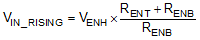
The EN rising threshold (VENH) for LMR23625 is set to be 1.55 V (typical). Choose the value of RENB to be 287 kΩ to minimize input current from the supply. If the desired VIN UVLO level is at 6.0 V, then the value of RENT can be calculated using Equation 20:
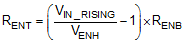
Equation 20 yields a value of 820 kΩ. The resulting falling UVLO threshold, equals 4.4 V, can be calculated by Equation 21, where EN hysteresis (VEN_HYS) is 0.4 V (typical).