ZHCS015G october   2011  – august 2023 BQ25504

PRODUCTION DATA  

  1.   1
  2. 特性
  3. 应用
  4. 说明
  5. Revision History
  6. 说明(续)
  7. Pin Configuration and Functions
  8. Specifications
    1. 7.1 Absolute Maximum Ratings
    2. 7.2 ESD Ratings
    3. 7.3 Recommended Operating Conditions
    4. 7.4 Thermal Information
    5. 7.5 Electrical Characteristics
    6. 7.6 Typical Characteristics
  9. Detailed Description
    1. 8.1 Overview
    2. 8.2 Functional Block Diagram
    3. 8.3 Feature Description
      1. 8.3.1 Maximum Power Point Tracking
      2. 8.3.2 Battery Undervoltage Protection
      3. 8.3.3 Battery Overvoltage Protection
      4. 8.3.4 Battery Voltage in Operating Range (VBAT_OK Output)
      5. 8.3.5 Nano-Power Management and Efficiency
    4. 8.4 Device Functional Modes
      1. 8.4.1 Cold-Start Operation (VSTOR < VSTOR_CHGEN, VIN_DC > VIN(CS) and PIN > PIN(CS))
      2. 8.4.2 Main Boost Charger Enabled (VSTOR > VSTOR_CHGEN, VIN_DC > VIN(DC) and EN = LOW )
      3. 8.4.3 Thermal Shutdown
  10. Application and Implementation
    1. 9.1 Application Information
      1. 9.1.1 Storage Element Selection
      2. 9.1.2 Inductor Selection
      3. 9.1.3 Capacitor Selection
        1. 9.1.3.1 VREF_SAMP Capacitance
        2. 9.1.3.2 VIN_DC Capacitance
        3. 9.1.3.3 VSTOR Capacitance
        4. 9.1.3.4 Additional Capacitance on VSTOR or VBAT
    2. 9.2 Typical Applications
      1. 9.2.1 Solar Application Circuit
        1. 9.2.1.1 Design Requirements
        2. 9.2.1.2 Detailed Design Procedure
        3. 9.2.1.3 Application Curves
      2. 9.2.2 TEG Application Circuit
        1. 9.2.2.1 Design Requirements
        2. 9.2.2.2 Detailed Design Procedure
        3. 9.2.2.3 Application Curves
      3. 9.2.3 MPPT Disabled, Low Impedance Source Application Circuit
        1. 9.2.3.1 Design Requirements
        2. 9.2.3.2 Detailed Design Procedure
        3. 9.2.3.3 Application Curves
  11. 10Power Supply Recommendations
  12. 11Layout
    1. 11.1 Layout Guidelines
    2. 11.2 Layout Example
    3. 11.3 Thermal Considerations
  13. 12Device and Documentation Support
    1. 12.1 Device Support
      1. 12.1.1 第三方产品免责声明
      2. 12.1.2 Zip Files
    2. 12.2 Documentation Support
      1. 12.2.1 Related Documentation
    3. 12.3 接收文档更新通知
    4. 12.4 支持资源
    5. 12.5 Trademarks
    6. 12.6 静电放电警告
    7. 12.7 术语表
  14. 13Mechanical, Packaging, and Orderable Information

封装选项

机械数据 (封装 | 引脚)
散热焊盘机械数据 (封装 | 引脚)
订购信息

Battery Voltage in Operating Range (VBAT_OK Output)

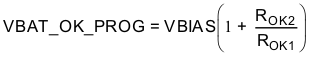
The IC allows the user to set a programmable voltage independent of the overvoltage and undervoltage settings to indicate whether the VSTOR voltage (and therefore the VBAT voltage when the PFET between the two pins is turned on) is at an acceptable level. When the battery voltage is decreasing the threshold is set by Equation 4:

Equation 4. GUID-8F9EB59F-4995-4093-B773-C4D4F4454F94-low.gif

When the battery voltage is increasing, the threshold is set by Equation 5:

Equation 5. GUID-C4031B53-71A4-4EEF-827B-49470C21FD97-low.gif

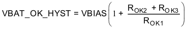
The sum of the resistors are recommended to be approximately 10 MΩ i.e., ROK1 + ROK2 + ROK3= 10 MΩ. Spreadsheet SLURAQ1 provides help on sizing and selecting the resistors.

The logic high level of this signal is equal to the VSTOR voltage and the logic low level is ground. The logic high level has ~20 KΩ internally in series to limit the available current to prevent MCU damage until it is fully powered. The VBAT_OK_PROG threshold must be greater than or equal to the UV threshold. Figure 8-1 shows the relative position of the various threshold voltages.

GUID-857120F3-1BD0-417E-A537-54888607A19D-low.gifFigure 8-1 Summary of VSTOR Threshold Voltages