ZHCS015G october   2011  – august 2023 BQ25504

PRODUCTION DATA  

  1.   1
  2. 特性
  3. 应用
  4. 说明
  5. Revision History
  6. 说明(续)
  7. Pin Configuration and Functions
  8. Specifications
    1. 7.1 Absolute Maximum Ratings
    2. 7.2 ESD Ratings
    3. 7.3 Recommended Operating Conditions
    4. 7.4 Thermal Information
    5. 7.5 Electrical Characteristics
    6. 7.6 Typical Characteristics
  9. Detailed Description
    1. 8.1 Overview
    2. 8.2 Functional Block Diagram
    3. 8.3 Feature Description
      1. 8.3.1 Maximum Power Point Tracking
      2. 8.3.2 Battery Undervoltage Protection
      3. 8.3.3 Battery Overvoltage Protection
      4. 8.3.4 Battery Voltage in Operating Range (VBAT_OK Output)
      5. 8.3.5 Nano-Power Management and Efficiency
    4. 8.4 Device Functional Modes
      1. 8.4.1 Cold-Start Operation (VSTOR < VSTOR_CHGEN, VIN_DC > VIN(CS) and PIN > PIN(CS))
      2. 8.4.2 Main Boost Charger Enabled (VSTOR > VSTOR_CHGEN, VIN_DC > VIN(DC) and EN = LOW )
      3. 8.4.3 Thermal Shutdown
  10. Application and Implementation
    1. 9.1 Application Information
      1. 9.1.1 Storage Element Selection
      2. 9.1.2 Inductor Selection
      3. 9.1.3 Capacitor Selection
        1. 9.1.3.1 VREF_SAMP Capacitance
        2. 9.1.3.2 VIN_DC Capacitance
        3. 9.1.3.3 VSTOR Capacitance
        4. 9.1.3.4 Additional Capacitance on VSTOR or VBAT
    2. 9.2 Typical Applications
      1. 9.2.1 Solar Application Circuit
        1. 9.2.1.1 Design Requirements
        2. 9.2.1.2 Detailed Design Procedure
        3. 9.2.1.3 Application Curves
      2. 9.2.2 TEG Application Circuit
        1. 9.2.2.1 Design Requirements
        2. 9.2.2.2 Detailed Design Procedure
        3. 9.2.2.3 Application Curves
      3. 9.2.3 MPPT Disabled, Low Impedance Source Application Circuit
        1. 9.2.3.1 Design Requirements
        2. 9.2.3.2 Detailed Design Procedure
        3. 9.2.3.3 Application Curves
  11. 10Power Supply Recommendations
  12. 11Layout
    1. 11.1 Layout Guidelines
    2. 11.2 Layout Example
    3. 11.3 Thermal Considerations
  13. 12Device and Documentation Support
    1. 12.1 Device Support
      1. 12.1.1 第三方产品免责声明
      2. 12.1.2 Zip Files
    2. 12.2 Documentation Support
      1. 12.2.1 Related Documentation
    3. 12.3 接收文档更新通知
    4. 12.4 支持资源
    5. 12.5 Trademarks
    6. 12.6 静电放电警告
    7. 12.7 术语表
  14. 13Mechanical, Packaging, and Orderable Information

封装选项

机械数据 (封装 | 引脚)
散热焊盘机械数据 (封装 | 引脚)
订购信息

Application Curves

GUID-874D5CD1-C64F-4BEF-9462-1395E23250FA-low.png
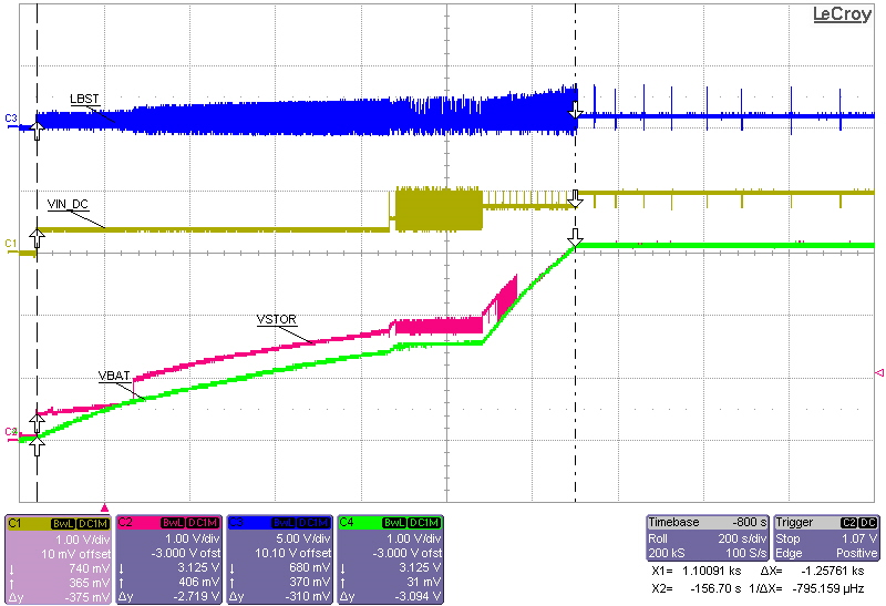
VINDC = sourcemeter with VSOURCE = 1.0 V and compliance of 2.75 mA
VBAT connected to 0.1 F depleted supercap
No resistance load on VSTOR
Figure 9-2 Startup into Depleted Storage Element
GUID-4A299CE8-48FF-4E1A-A3E4-B4BFA53DA91E-low.png
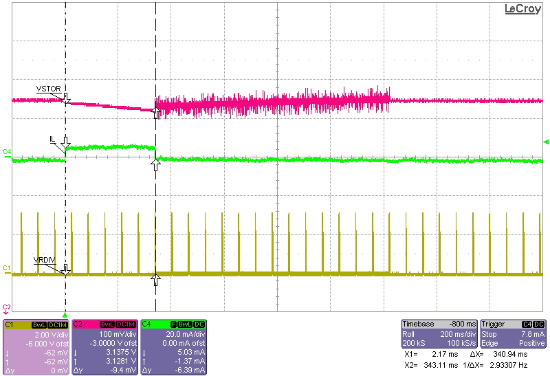
VIN_DC = sourcemeter with VSOURCE = 1 V and compliance of 10.5 mA
VBAT = 0.1 F supercap
VSTOR = open to 500 Ω to open resistive load (IL = load current on VSTOR)
Figure 9-4 5 mA Load Transient on VSTOR
GUID-05A1B637-F952-4428-BED5-977F91D0F9CB-low.png
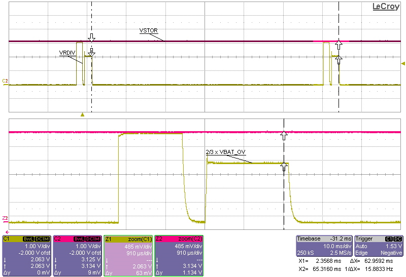
VIN_DC = sourcemeter with VSOURCE = 1 V and compliance of 10.5 mA
VBAT = sourcemeter with VSOURCE = 2.8 V and compliance of 1A
Figure 9-6 VRDIV Operation
GUID-F90825EB-AC67-4ED4-8477-F15D10CD8F95-low.png
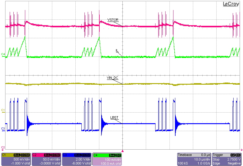
VIN_DC = sourcemeter with VSOURCE = 1 V and compliance of 10.5 mA
VBAT = 0.1 F supercap
VSTOR = 2 kΩ resistive load
Figure 9-3 Boost Charger Operational Waveforms
GUID-17329618-6452-427D-8D89-6B5A86AC2DE2-low.png
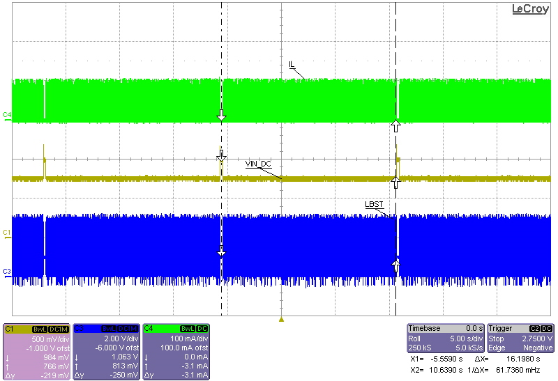
VIN_DC = sourcemeter with VSOURCE = 1 V and compliance of 10.5 mA
VBAT = sourcemeter with VSOURCE = 2.8V and compliance of 1A
IL = inductor current
Figure 9-5 MPPT Operation
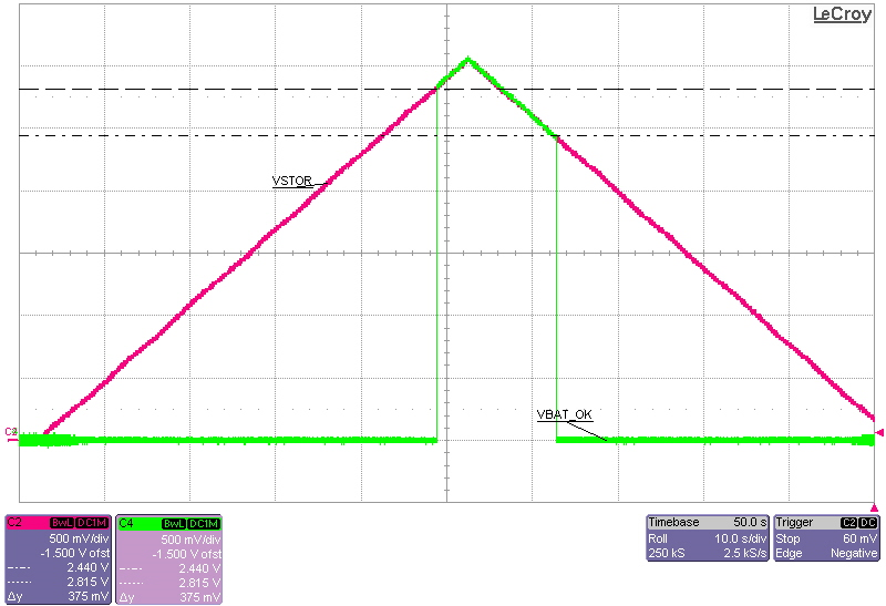
GUID-3B45A29E-EED6-4F5A-9C03-5E46B6E19898-low.png
VIN_DC = sourcemeter with VSOURCE = 1 V and compliance of 2.75 mA
No storage element on VBAT
VSTOR artificially ramped from 0V to 3.15 V to 0 V using a power amp driven by a function generator
Figure 9-7 VBAT_OK Operation