ZHCSGU6A september 2017 – july 2023 ADS8588H
PRODUCTION DATA
- 1
- 1 特性
- 2 应用
- 3 说明
- 4 Revision History
- 5 Pin Configuration and Functions
-
6 Specifications
- 6.1 Absolute Maximum Ratings
- 6.2 ESD Ratings
- 6.3 Recommended Operating Conditions
- 6.4 Thermal Information
- 6.5 Electrical Characteristics
- 6.6 Timing Requirements: CONVST Control
- 6.7 Timing Requirements: Data Read Operation
- 6.8 Timing Requirements: Parallel Data Read Operation, CS and RD Tied Together
- 6.9 Timing Requirements: Parallel Data Read Operation, CS and RD Separate
- 6.10 Timing Requirements: Serial Data Read Operation
- 6.11 Timing Requirements: Byte Mode Data Read Operation
- 6.12 Timing Requirements: Oversampling Mode
- 6.13 Timing Requirements: Exit Standby Mode
- 6.14 Timing Requirements: Exit Shutdown Mode
- 6.15 Switching Characteristics: CONVST Control
- 6.16 Switching Characteristics: Parallel Data Read Operation, CS and RD Tied Together
- 6.17 Switching Characteristics: Parallel Data Read Operation, CS and RD Separate
- 6.18 Switching Characteristics: Serial Data Read Operation
- 6.19 Switching Characteristics: Byte Mode Data Read Operation
- 6.20 Timing Diagrams
- 6.21 Typical Characteristics
-
7 Detailed Description
- 7.1 Overview
- 7.2 Functional Block Diagram
- 7.3 Feature Description
- 7.4
Device Functional Modes
- 7.4.1
Device Interface: Pin Description
- 7.4.1.1 REFSEL (Input)
- 7.4.1.2 RANGE (Input)
- 7.4.1.3 STBY (Input)
- 7.4.1.4 PAR/SER/BYTE SEL (Input)
- 7.4.1.5 CONVSTA, CONVSTB (Input)
- 7.4.1.6 RESET (Input)
- 7.4.1.7 RD/SCLK (Input)
- 7.4.1.8 CS (Input)
- 7.4.1.9 OS[2:0]
- 7.4.1.10 BUSY (Output)
- 7.4.1.11 FRSTDATA (Output)
- 7.4.1.12 DB15/BYTE SEL
- 7.4.1.13 DB14/HBEN
- 7.4.1.14 DB[13:9]
- 7.4.1.15 DB8/DOUTB
- 7.4.1.16 DB7/DOUTA
- 7.4.1.17 DB[6:0]
- 7.4.2 Device Modes of Operation
- 7.4.1
Device Interface: Pin Description
- 8 Application and Implementation
- 9 Device and Documentation Support
- 10Mechanical, Packaging, and Orderable Information
8.2.2 Detailed Design Procedure
For the ADS8588H, each channel incorporates an analog front-end composed of a programmable gain amplifier (PGA), analog low-pass filter, and ADC input driver. The analog input for each channel presents a constant resistive impedance of 1 MΩ independent of the ADC sampling frequency and range setting. The high input impedance of the analog front-end circuit allows direct connection to potential transformers (PT) and current transformers (CT). The ADC inputs can support up to ±10-V or ± 5-V bipolar inputs and the integrated signal conditioning eliminates the need for external amplifiers or ADC driver circuits.
The PT and CT used in the system (Figure 8-1) have a ±10-V output range. Although the PT and CT provide isolation from the power system, a series resistor must be placed on the analog input channels. The series resistor helps limit the input current to ±10 mA if the input voltages exceed ±15 V. For applications that require protection against overvoltage or fast transient events beyond the specified absolute maximum ratings of the device, an external protection clamp circuit using transient voltage suppressors (TVS) and ESD diodes is recommended.
A low-pass filter is used on each analog input channel to eliminate high-frequency noise pickup and minimize aliasing. Figure 8-2 shows an example of the recommended configuration for an input RC filter. A balanced RC filter configuration matches the external source resistance on the positive path (AIN_nP) with an equal resistance on the negative path (AIN_nGND). Matching the source impedance in the positive and negative path allows for better common-mode noise rejection and helps maintain the dc accuracy of the system by canceling any additional offset error contributed by the external series resistance.
 Figure 8-2 Input RC Low-Pass Filter
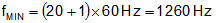
The primary goal of the data acquisition system illustrated in Figure 8-1 is to measure up to 20 harmonics in a 60-Hz power network. Thus, the analog front-end must have sufficient bandwidth to detect signals up to 1260 Hz, as shown in Equation 1.
Based on the bandwidth calculated in Equation 1, the ADS8588H is set to simultaneously sample all eight channels at 20 kSPS, which is sufficient throughput to clearly resolve the highest harmonic component of the input signal. The pass band of the low-pass filter configuration shown in Figure 8-2 is determined by the –3-dB frequency, calculated according to Equation 2.

The value of CF is selected as 5.6 nF, a standard capacitance value available in 0603-size surface-mount components. In combination with the resistor RF, this low-pass filter provides sufficient bandwidth to accommodate the required 20 harmonics for the input signal of 60 Hz.
The ADS8588H can operate with either the internal voltage reference or an external reference. The Internal Reference section describes the electrical connections and recommended bypass capacitors when using the internal reference. Alternatively for applications that require a higher precision voltage reference, Figure 8-3 illustrates an example of an external reference circuit. The REF5025 provides a very low drift, and very accurate external 2.5-V reference. The resistor RFILT and capacitor CFILT form a low-pass filter to reduce the broadband noise and minimize the resulting effect of the reference noise on the system performance.
 Figure 8-3 External Reference Circuit for the ADS8588H