ZHCSGU6A september 2017 – july 2023 ADS8588H
PRODUCTION DATA
- 1
- 1 特性
- 2 应用
- 3 说明
- 4 Revision History
- 5 Pin Configuration and Functions
-
6 Specifications
- 6.1 Absolute Maximum Ratings
- 6.2 ESD Ratings
- 6.3 Recommended Operating Conditions
- 6.4 Thermal Information
- 6.5 Electrical Characteristics
- 6.6 Timing Requirements: CONVST Control
- 6.7 Timing Requirements: Data Read Operation
- 6.8 Timing Requirements: Parallel Data Read Operation, CS and RD Tied Together
- 6.9 Timing Requirements: Parallel Data Read Operation, CS and RD Separate
- 6.10 Timing Requirements: Serial Data Read Operation
- 6.11 Timing Requirements: Byte Mode Data Read Operation
- 6.12 Timing Requirements: Oversampling Mode
- 6.13 Timing Requirements: Exit Standby Mode
- 6.14 Timing Requirements: Exit Shutdown Mode
- 6.15 Switching Characteristics: CONVST Control
- 6.16 Switching Characteristics: Parallel Data Read Operation, CS and RD Tied Together
- 6.17 Switching Characteristics: Parallel Data Read Operation, CS and RD Separate
- 6.18 Switching Characteristics: Serial Data Read Operation
- 6.19 Switching Characteristics: Byte Mode Data Read Operation
- 6.20 Timing Diagrams
- 6.21 Typical Characteristics
-
7 Detailed Description
- 7.1 Overview
- 7.2 Functional Block Diagram
- 7.3 Feature Description
- 7.4
Device Functional Modes
- 7.4.1
Device Interface: Pin Description
- 7.4.1.1 REFSEL (Input)
- 7.4.1.2 RANGE (Input)
- 7.4.1.3 STBY (Input)
- 7.4.1.4 PAR/SER/BYTE SEL (Input)
- 7.4.1.5 CONVSTA, CONVSTB (Input)
- 7.4.1.6 RESET (Input)
- 7.4.1.7 RD/SCLK (Input)
- 7.4.1.8 CS (Input)
- 7.4.1.9 OS[2:0]
- 7.4.1.10 BUSY (Output)
- 7.4.1.11 FRSTDATA (Output)
- 7.4.1.12 DB15/BYTE SEL
- 7.4.1.13 DB14/HBEN
- 7.4.1.14 DB[13:9]
- 7.4.1.15 DB8/DOUTB
- 7.4.1.16 DB7/DOUTA
- 7.4.1.17 DB[6:0]
- 7.4.2 Device Modes of Operation
- 7.4.1
Device Interface: Pin Description
- 8 Application and Implementation
- 9 Device and Documentation Support
- 10Mechanical, Packaging, and Orderable Information
7.4.2.2.2 Simultaneous Sampling Two Sets of Input Channels
The ADS8588H allows two sets of analog input channels to be simultaneously sampled. In order to do so, the CONVSTA and CONVSTB signals must be separate control inputs (as shown in Figure 7-17) and the device must not operate in any oversampling mode. Electrical grid relay protection is an application that can benefit from being able to sample the inputs in two groups. The delay of the signal through the voltage channels is often different from the delay on the channels measuring current. The difference in delay created by the voltage and current signal paths can be corrected by adjusting the sampling of the two groups of inputs (voltage and current) to the device.
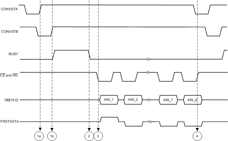
The timing diagram in Figure 7-17 shows the sequence of events described in this section.
 Figure 7-17 Simultaneous Sampling of All Input Channels in Parallel Interface Timing Diagram
There are four events that describe the internal operation of the device when pairs of input channels are simultaneously sampled and the data are read back. These events are:
- Event 1(a): A rising edge on the CONVSTA signal initiates simultaneous sampling of the first set of analog input channels (channels 1-4 for the ADS8588H). The sampling circuits on the first set of analog input channels enter hold mode and the input signals on these channels are sampled at the same instant. The ADC does not begin conversion until the input signals on the second set of channels are sampled.
- Event 1(b): A rising edge on the CONVSTB signal initiates simultaneous sampling of the second set of analog input channels (channels 5-8 for the ADS8588H). The sampling circuits for the second set of analog input channels enter hold mode and the input signals on these channels are sampled at the same instant. When the rising edges of both the CONVSTA and CONVSTB signals have occurred, the ADC converts all sampled signals using a precise, on-chip oscillator clock. At the beginning of the conversion phase of the ADC, the BUSY output goes high and remains high through a maximum-specified conversion time of tCONV (see the Timing Requirements: CONVST ControlTiming Requirements: CONVST Control table).
- Event 2: Same as event 2 in the Simultaneous Sampling on All Input Channels section.
- Event 3: Same as event 3 in the Simultaneous Sampling on All Input Channels section.
- Event 4: Same as event 4 in the Simultaneous Sampling on All Input Channels section.
Events 1(a), 1(b), and 2 are common to all interface modes of operation (parallel, serial, or parallel byte).